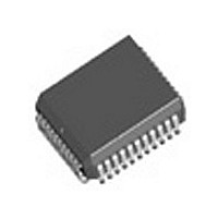
IDT72V8981J8 IDT, Integrated Device Technology Inc, IDT72V8981J8 Datasheet - Page 7

IDT72V8981J8
Manufacturer Part Number
IDT72V8981J8
Description
IC DGTL SW 128X128 44-PLCC
Manufacturer
IDT, Integrated Device Technology Inc
Series
72Vr
Type
Multiplexerr
Datasheet
1.IDT72V8981J8.pdf
(11 pages)
Specifications of IDT72V8981J8
Circuit
1 x 4:4
Independent Circuits
1
Voltage Supply Source
Single Supply
Voltage - Supply
3 V ~ 3.6 V
Operating Temperature
-40°C ~ 85°C
Mounting Type
Surface Mount
Package / Case
44-PLCC
Lead Free Status / RoHS Status
Contains lead / RoHS non-compliant
Current - Output High, Low
-
Lead Free Status / RoHS Status
Not Compliant, Contains lead / RoHS non-compliant
Other names
72V8981J8
Available stocks
Company
Part Number
Manufacturer
Quantity
Price
Company:
Part Number:
IDT72V8981J8
Manufacturer:
IDT, Integrated Device Technology Inc
Quantity:
10 000
ABSOLUTE MAXIMUM RATINGS
DC ELECTRICAL CHARACTERISTICS
NOTE:
1. Typical figures are at 25°C and are for design aid only; not guaranteed and not subject to production testing.
NOTE:
1. Stresses greater than those listed under ABSOLUTE MAXIMUM RATINGS may cause
permanent damage to the device. This is a stress rating only and functional operation of
the device at these or any other conditions above those indicated in the operational sections
of this specification is not implied. Exposure to absolute maximum rating conditions for
extended periods may affect reliability.
IDT72V8981 3.3V Time Slot Interchange
Digital Switch 128 x 128
Symbol
Vcc
V
P
Symbol
T
Vi
I
O
S
O
D
V
V
V
I
I
C
I
V
I
I
C
CC
OH
OL
OZ
OH
IL
OL
IH
IL
O
I
Output
Pin
Parameter
Symbol Voltage
Voltage on Digital Inputs
Voltage on Digital Outputs
Current at Digital Outputs
Storage Temperature
Package Power Dissapation
Parameter
Supply Current
Input High Voltage
Input Low Voltage
Input Leakage
Input Capacitance
Output High Voltage
Output High Current
Output Low Voltage
Output Low Current
High Impedance Leakage
Output Pin Capacitance
C
Figure 4. Output Load
L
Test Point
GND
S
GND - 0.3
GND - 0.3
1
Min.
-0.3
-55
R
L
V
V
CC
CC
Max.
+125
20
5
1
+0.5
+0.3
Min.
2.0
2.4
10
5
(1)
5702 drw08
Unit
mA
° C
GND
W
V
V
V
S
VCC
2
7
Typ.
RECOMMENDED OPERATING
CONDITIONS
NOTE:
1. Typical figures are at 25°C and are for design aid only; not guaranteed and not subject
S1 is open circuit except when testing
output levels or high impedance states.
S2 is switched to V
testing output levels or high impedance
states.
3
Symbol
to production testing.
V
V
T
(1)
OP
CC
I
Positive Supply
Input Voltage
Operating Temperature
Commercial
Max.
0.8
0.4
15
10
5
5
Parameter
CC
or GND when
Units
Commercial Temperature Range
mA
µA
mA
mA
µA
pF
pF
V
V
V
V
3.0
-40
Min.
0
V
V
O
I
Sourcing. V
between GND and V
Sinking. V
between GND and V
Typ.
Outputs Unloaded
Test Conditions
25
I
OH
I
(1)
OL
= 10mA
= 5mA
Max.
OL
5.25
+85
OH
3.6
= 0.4V
= 2.4V
Unit
CC
°C
CC
V
V


