11LC160-I/P Microchip Technology, 11LC160-I/P Datasheet - Page 10

11LC160-I/P
Manufacturer Part Number
11LC160-I/P
Description
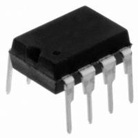
IC EEPROM 16KBIT 100KHZ 8DIP
Manufacturer
Microchip Technology
Datasheets
1.11LC010T-ITT.pdf
(44 pages)
2.11LC010T-ITT.pdf
(22 pages)
3.11LC010T-ITT.pdf
(6 pages)
4.11LC160T-ITT.pdf
(38 pages)
Specifications of 11LC160-I/P
Memory Size
16K (2K x 8)
Package / Case
8-DIP (0.300", 7.62mm)
Operating Temperature
-40°C ~ 85°C
Format - Memory
EEPROMs - Serial
Memory Type
EEPROM
Speed
100kHz
Interface
UNI/O™ (Single Wire)
Voltage - Supply
2.5 V ~ 5.5 V
Organization
2048 x 8
Interface Type
Serial
Maximum Clock Frequency
100 KHz
Supply Voltage (max)
5.5 V
Supply Voltage (min)
2.5 V
Maximum Operating Current
50 uA
Maximum Operating Temperature
+ 85 C
Mounting Style
Through Hole
Minimum Operating Temperature
- 40 C
Operating Supply Voltage
3.3 V, 5 V
Lead Free Status / RoHS Status
Lead free / RoHS Compliant
Lead Free Status / RoHS Status
Lead free / RoHS Compliant, Lead free / RoHS Compliant
UNI/O
4.0
Clock and data are embedded together through Man-
chester encoding. Each data bit is transmitted within a
single bit period, T
during the start header of the command.
Every bit period includes an edge transition at the mid-
dle of the period, and it is the direction of this edge
which determines the value of the bit. A rising middle
edge indicates a ‘1’ value, whereas a falling edge
indicates a ‘0’, as shown in Figure 4-1.
FIGURE 4-1:
Because every bit period must have a middle edge
transition, there may or may not exist another edge
transition at the beginning of a bit period. This is
entirely dependent upon the values of both the previ-
ous and current bits. If two bits of equal value are
being successively transmitted, then a transition at the
beginning of the second bit is required. If the two bits
are of opposing values, then no edge will occur. Refer
to Figure 4-2 for details.
DS22076D-page 10
BIT-LEVEL DEFINITION
T
‘1’
E
®
E
Bus
, which is specified by the master
BIT VALUES
T
‘0’
E
FIGURE 4-2:
4.1
In order to allow for flexibility in timing, UNI/O bus-
compatible devices must be tolerant of small devia-
tions, or jitter, in input edge timing, as specified by
T
Slave devices must also allow for a small amount of
frequency drift. F
byte tolerance required for all slave devices, and F
shows the overall drift from the initial serial bit period
for a single command. For example, if a command is
begun using a 20 µs bit period, the master can drift a
maximum of 20 µs*F
µs*F
IJIT
. See Figure 12-4 for details.
DEV
Timing Considerations
within that command.
‘1’
‘1’
DRIFT
No Edge Exists
DRIFT
Edge Exists
SUCCESSIVE BIT
TRANSMISSION
EXAMPLE
specifies the maximum drift per
© 2009 Microchip Technology Inc.
per byte, up to a total of 20
‘1’
‘0’
DEV


