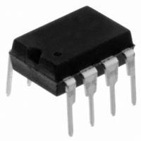
11LC160-I/P Microchip Technology, 11LC160-I/P Datasheet - Page 8

11LC160-I/P
Manufacturer Part Number
11LC160-I/P
Description
IC EEPROM 16KBIT 100KHZ 8DIP
Manufacturer
Microchip Technology
Datasheets
1.11LC010T-ITT.pdf
(44 pages)
2.11LC010T-ITT.pdf
(22 pages)
3.11LC010T-ITT.pdf
(6 pages)
4.11LC160T-ITT.pdf
(38 pages)
Specifications of 11LC160-I/P
Memory Size
16K (2K x 8)
Package / Case
8-DIP (0.300", 7.62mm)
Operating Temperature
-40°C ~ 85°C
Format - Memory
EEPROMs - Serial
Memory Type
EEPROM
Speed
100kHz
Interface
UNI/O™ (Single Wire)
Voltage - Supply
2.5 V ~ 5.5 V
Organization
2048 x 8
Interface Type
Serial
Maximum Clock Frequency
100 KHz
Supply Voltage (max)
5.5 V
Supply Voltage (min)
2.5 V
Maximum Operating Current
50 uA
Maximum Operating Temperature
+ 85 C
Mounting Style
Through Hole
Minimum Operating Temperature
- 40 C
Operating Supply Voltage
3.3 V, 5 V
Lead Free Status / RoHS Status
Lead free / RoHS Compliant
Lead Free Status / RoHS Status
Lead free / RoHS Compliant, Lead free / RoHS Compliant
UNI/O
2.0
There is only a single I/O signal, SCIO, necessary for
communication between devices and all data trans-
mission occurs through this line. The SCIO signal for
all devices in a system are connected together directly
in a bussed configuration. The Idle state of the bus is
high. In order to ensure the bus is in the Idle state dur-
ing times when the master may not be driving the bus,
the use of a pull-up resistor is recommended. Both
clock and data are embedded together by way of
Manchester encoding.
The serial stream is divided into bit periods, with one
data bit being embedded per period. The bit period
time is determined by the master and communicated
to the slave during the start header at the beginning of
each command. Therefore, the bit period must only be
consistent within a single command.
2.1
Parameter F
supported frequency range. Note that, due to the
asynchronous nature of the bus, both minimum and
maximum frequencies are defined.
2.2
In order to support a wide number of fabrication pro-
cesses, no limitation has been defined for the operat-
ing voltages of devices attached to the bus. Such
ranges are dependent solely on the specific devices.
The only requirement is that input threshold voltages
and output current limits meet the electrical specifica-
tions set forth in Table 12-1.
2.3
The I/O structure for SCIO consists of an input buffer
and a tri-stateable, push-pull output driver. To avoid
high currents during possible bus contention, and to
refrain from requiring external components, the SCIO
output driver on all slave devices must be current-lim-
ited to the specifications listed in Table 12-1. If the out-
put driver on the master device in a system is not
significantly stronger than on the slave devices,
ambiguous voltage levels may occur during times of
possible bus contention.
Because the bus Idle state is high, a pull-up resistor is
recommended to ensure bus idle during power
up/down sequences, as well as any other time in
which no device is driving the bus.
DS22076D-page 8
GENERAL CHARACTERISTICS
Bit Rate
Voltage Range
I/O Structures
BIT
®
in Table 12-2 defines the currently
Bus
2.4
Successful communication is dependant upon edge
transitions occurring within the proper time frames.
Moreover, slew rates must be minimized to avoid
detecting unwanted edges, most critically during the
start header. Because of this, the bus capacitance is
limited to 100 pF. This is comprised of the SCIO pin
capacitance for all devices on the bus, as well as the
capacitance of all wires and connections.
2.5
The UNI/O bus is not designed for any particular pro-
cess or technology. Therefore, all IC fabrication tech-
nologies are supported, so long as the electrical
specifications set forth in Section 12.0 “Electrical
Specifications” are met.
Bus Capacitance
Fabrication Processes
© 2009 Microchip Technology Inc.


