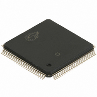
CY7C038V-15AC Cypress Semiconductor Corp, CY7C038V-15AC Datasheet

CY7C038V-15AC
Specifications of CY7C038V-15AC
Available stocks
Related parts for CY7C038V-15AC
CY7C038V-15AC Summary of contents
Page 1
... CMOS for optimum speed/power • High-speed access: 15/20/25 ns • Low operating power — Active: I ...
Page 2
... Two ports are provided, permitting independent, asynchro- nous access for reads and writes to any location in memory. The devices can be utilized as stand-alone 16/18-bit dual-port static RAMs or multiple devices can be combined in order to function as a 32/36-bit or wider master/slave dual-port static RAM ...
Page 3
... Typical Standby Current for I (mA) (Both ports SB1 TTL level) Typical Standby Current for (Both ports SB3 CMOS level) Note: 6. This pin is NC for CY7C037V. 100-Pin TQFP (Top View CY7C038V (64K x 18) CY7C037V (32K x 18 CY7C027V/028V CY7C037V/038V -15 15 125 CY7C027V/028V CY7C037V/038V ...
Page 4
... Power Applied .............................................– +125 C Supply Voltage to Ground Potential ............... –0.5V to +4.6V DC Voltage Applied to Outputs in High Z State ...........................–0. Note: 7. Pulse width < 20 ns. 8. Industrial parts are available in CY7C028V and CY7C038V only. Description Chip Enable (CE is LOW when CE 0 Read/Write Enable Output Enable Address (A –A for 32K ...
Page 5
Electrical Characteristics Over the Operating Range Symbol Parameter V Output HIGH Voltage OH (V =Min –4.0 mA Output LOW Voltage (V =Min Input HIGH Voltage IH V Input LOW Voltage IL ...
Page 6
Switching Characteristics Over the Operating Range Parameter Description READ CYCLE t Read Cycle Time RC t Address to Data Valid AA t Output Hold From Address Change OHA [12 LOW to Data Valid ACE t OE LOW to ...
Page 7
Switching Characteristics Over the Operating Range Parameter Description [17] INTERRUPT TIMING t INT Set Time INS t INT Reset Time INR SEMAPHORE TIMING t SEM Flag Update Pulse (OE or SEM) SOP t SEM Flag Write to Read Time SWRD ...
Page 8
Switching Waveforms Read Cycle No. 1 (Either Port Address Access) ADDRESS OHA DATA OUT PREVIOUS DATA VALID Read Cycle No. 2 (Either Port CE/OE Access) CE and DATA OUT I CC CURRENT I ...
Page 9
Switching Waveforms (continued) Write Cycle No. 1: R/W Controlled Timing ADDRESS OE [29,30 R/W NOTE 32 DATA OUT DATA IN Write Cycle No Controlled Timing ADDRESS [29,30 R/W DATA IN Notes: 25. ...
Page 10
Switching Waveforms (continued) Semaphore Read After Write Timing, Either Side A –A VALID ADRESS SEM I R/W OE Timing Diagram of Semaphore Contention A – R/W L SEM L A –A ...
Page 11
Switching Waveforms (continued) Timing Diagram of Read with BUSY (M/S=HIGH) ADDRESS R R/W R DATA ADDRESS L BUSY L DATA OUTL Write Timing with Busy Input (M/S=LOW) R/W BUSY Note: 38 LOW. ...
Page 12
Switching Waveforms (continued) Busy Timing Diagram No. 1 (CE Arbitration) CE Valid First: L ADDRESS L BUSY R CE Valid First: R ADDRESS L BUSY L Busy Timing Diagram No. 2 (Address ...
Page 13
Switching Waveforms (continued) Interrupt Timing Diagrams Left Side Sets INT : R ADDRESS WRITE 7FFF (FFFF for CY7C028V/38V R/W L INT R [41] t INS Right Side Clears INT : R ADDRESS R/W R ...
Page 14
... HIGH during SEM LOW). A address. OE and R/W are used in the same manner as a normal memory access. When writing or reading a semaphore, the other address pins have no effect. When writing to the semaphore, only I/O written to the left port of an available semaphore, a one will appear at the same semaphore address on the right port ...
Page 15
Table 1. Non-Contending Read/Write Inputs CE R ...
Page 16
... Asynchronous Dual-Port SRAM Speed (ns) Ordering Code 15 CY7C037V-15AC 20 CY7C037V-20AC 25 CY7C037V-25AC 64K x18 3.3V Asynchronous Dual-Port SRAM Speed (ns) Ordering Code 15 CY7C038V-15AC 20 CY7C038V-20AC CY7C038V-20AI 25 CY7C038V-25AC Document #: 38–00670–*D Package Name Package Type A100 100-Pin Thin Quad Flat Pack A100 100-Pin Thin Quad Flat Pack A100 ...
Page 17
... Package Diagram © Cypress Semiconductor Corporation, 2000. The information contained herein is subject to change without notice. Cypress Semiconductor Corporation assumes no responsibility for the use of any circuitry other than circuitry embodied in a Cypress Semiconductor product. Nor does it convey or imply any license under patent or other rights. Cypress Semiconductor does not authorize its products for use as critical components in life-support systems where a malfunction or failure may reasonably be expected to result in significant injury to the user ...


