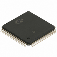
CY7C038V-15AXC Cypress Semiconductor Corp, CY7C038V-15AXC Datasheet

CY7C038V-15AXC
Specifications of CY7C038V-15AXC
Available stocks
Related parts for CY7C038V-15AXC
CY7C038V-15AXC Summary of contents
Page 1
... CMOS for optimum speed and power ■ High speed access: 15, 20, and 25 ns ■ Low operating power ■ ...
Page 2
Pin Configurations 100 A9L 1 A10L 2 A11L 3 A12L 4 A13L 5 A14L 6 [1] A15L LBL 10 UBL 11 CE0L 12 CE1L 13 CY7C027V/027VN/027AV (32K x 16) SEML 14 VCC ...
Page 3
... TTL level) SB1 Typical Standby Current for I (Both ports CMOS level) SB3 Note 2. This pin is NC for CY7C037V/037AV. Document #: 38-06078 Rev. *B CY7C027V/027VN/027AV/028V Figure 2. 100-Pin TQFP (Top View CY7C038V (64K x 18) CY7C037V/037AV (32K x 18 -15 15 125 35 10 μA CY7C037V/037AV/038V 80 79 ...
Page 4
... RAM cells, I/O and address lines, and control signals (CE, OE, R/W). These control pins permit independent access for reads or writes to any location in memory. To handle simultaneous writes/reads to the same location, a BUSY pin is provided on each port. Two interrupt (INT) pins can be utilized for port-to-port communication ...
Page 5
... Semaphores are accessed by asserting SEM LOW. The SEM pin and functions as a chip select for the semaphore latches (CE must remain HIGH during SEM LOW). A and R/W are used in the same manner as a normal memory access. of each other, PS When writing or reading a semaphore, the other address pins have no ...
Page 6
... Input Capacitance IN C Output Capacitance OUT Notes 2. Pulse width < 20 ns. 3. Industrial parts are available in CY7C028V and CY7C038V only 1/t = All inputs cycling 1/t (except output enable means no address or control lines change. This applies only to inputs at CMOS level standby I MAX ...
Page 7
R1 = 590Ω OUTPUT 435Ω (a) Normal Load (Load 1) 3.0V GND Switching Characteristics Over the Operating Range Parameter Description Read Cycle t Read Cycle Time RC t Address to Data Valid AA ...
Page 8
Switching Characteristics Over the Operating Range Parameter Description t Data Hold From Write End HD [9, 10] t R/W LOW to High Z HZWE [9 ,10] t R/W HIGH to Low Z LZWE [36] t Write Pulse to Data Delay ...
Page 9
Switching Waveforms Figure 4. Read Cycle No. 1 (Either Port Address Access) ADDRESS OHA DATA OUT PREVIOUS DATA VALID Figure 5. Read Cycle No. 2 (Either Port CE/OE Access) CE and DATA OUT ...
Page 10
Switching Waveforms (continued) Figure 7. Write Cycle No. 1: R/W Controlled Timing ADDRESS OE [24,25 R/W NOTE 27 DATA OUT DATA IN Figure 8. Write Cycle No Controlled Timing ADDRESS [24,25 R/W ...
Page 11
Switching Waveforms (continued) Figure 9. Semaphore Read After Write Timing, Either Side A –A VALID ADRESS SEM I R/W OE Figure 10. Timing Diagram of Semaphore Contention A – R/W L ...
Page 12
Switching Waveforms (continued) Figure 11. Timing Diagram of Read with BUSY (M/S=HIGH) ADDRESS R R/W R DATA ADDRESS L BUSY L DATA OUTL Figure 12. Write Timing with Busy Input (M/S=LOW) R/W BUSY Note 33. CE ...
Page 13
Switching Waveforms (continued) Figure 13. Busy Timing Diagram No. 1 (CE Arbitration) CE Valid First: L ADDRESS L BUSY R CE Valid First: R ADDRESS L BUSY L Figure 14. Busy Timing ...
Page 14
Switching Waveforms (continued) Left Side Sets INT : R ADDRESS WRITE 7FFF (FFFF for CY7C028V/38V R/W L INT R [36] t INS Right Side Clears INT : R ADDRESS R INT ...
Page 15
Table 1. Non-Contending Read/Write Inputs CE R ...
Page 16
... Ordering Code 15 CY7C037V-15AC CY7C037V-15AXC 20 CY7C037V-20AC CY7C037AV-20AXC 25 CY7C037V-25AC CY7C037V-25AXC 64K x18 3.3V Asynchronous Dual-Port SRAM Speed (ns) Ordering Code 15 CY7C038V-15AC CY7C038V-15AXC 20 CY7C038V-20AC CY7C038V-20AXC CY7C038V-20AI CY7C038V-20AXI 25 CY7C038V-25AC CY7C038V-25AXC Document #: 38-06078 Rev. *B CY7C027V/027VN/027AV/028V Package Name Package Type A100 100-Pin Thin Quad Flat Pack A100 ...
Page 17
Package Diagram Figure 16. 100-Pin Pb-Free Thin Plastic Quad Flat Pack (TQFP) A100 Document #: 38-06078 Rev. *B CY7C027V/027VN/027AV/028V CY7C037V/037AV/038V 51-85048-*C Page [+] Feedback ...
Page 18
... Cypress against all charges. Any Source Code (software and/or firmware) is owned by Cypress Semiconductor Corporation (Cypress) and is protected by and subject to worldwide patent protection (United States and foreign), United States copyright laws and international treaty provisions. Cypress hereby grants to licensee a personal, non-exclusive, non-transferable license to copy, use, modify, create derivative works of, and compile the Cypress Source Code and derivative works for the sole purpose of creating custom software and or firmware in support of licensee product to be used only in conjunction with a Cypress integrated circuit as specified in the applicable agreement ...


