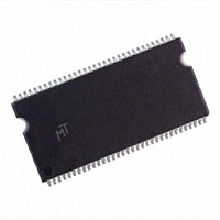
MT46V64M16TG-6T:A TR Micron Technology Inc, MT46V64M16TG-6T:A TR Datasheet - Page 7

MT46V64M16TG-6T:A TR
Manufacturer Part Number
MT46V64M16TG-6T:A TR
Description
IC DDR SDRAM 1GBIT 6NS 66TSOP
Manufacturer
Micron Technology Inc
Type
DDR SDRAMr
Datasheet
1.MT46V256M4P-6TA_TR.pdf
(82 pages)
Specifications of MT46V64M16TG-6T:A TR
Format - Memory
RAM
Memory Type
DDR SDRAM
Memory Size
1G (64M x 16)
Speed
6ns
Interface
Parallel
Voltage - Supply
2.3 V ~ 2.7 V
Operating Temperature
0°C ~ 70°C
Package / Case
66-TSOP
Organization
64Mx16
Density
1Gb
Address Bus
16b
Access Time (max)
700ps
Maximum Clock Rate
333MHz
Operating Supply Voltage (typ)
2.5V
Package Type
TSOP
Operating Temp Range
0C to 70C
Operating Supply Voltage (max)
2.7V
Operating Supply Voltage (min)
2.3V
Supply Current
275mA
Pin Count
66
Mounting
Surface Mount
Operating Temperature Classification
Commercial
Lead Free Status / RoHS Status
Contains lead / RoHS non-compliant
Figure 4:
Figure 5:
PDF: 09005aef80a2f898/Source: 09005aef82a95a3a
1Gb_DDR_x4x8x16_D2.fm - 1Gb DDR: Rev. I, Core DDR: Rev. B 12/07 EN
128 Meg x 8 Functional Block Diagram
64 Meg x 16 Functional Block Diagram
BA0, BA1
BA0, BA1
A0–A13,
A0–A13,
RAS#
CAS#
WE#
CAS#
RAS#
CKE
CK#
WE#
CS#
CKE
CK#
CK
CS#
CK
16
16
Address
register
Address
register
Mode registers
Mode registers
Control
Control
logic
16
logic
16
counter
14
Refresh
14
counter
Refresh
10
11
2
2
13
13
address
2
address
2
Row-
MUX
Row-
MUX
Column-
counter/
control
address
Column-
counter/
14
Bank
address
logic
latch
control
14
Bank
logic
latch
decoder
address
Bank 0
decoder
address
row-
latch
Bank 0
row-
latch
&
&
9
1
10
1
16,384
16,384
7
SENSE AMPLIFIERS
(16,384 x 512 x 32)
(16,384 x 1,024 x 16)
SENSE AMPLIFIERS
DM mask logic
DM mask logic
I/O gating
Column
decoder
I/O gating
memory
Bank 0
decoder
memory
Column
array
512
Bank 0
Bank 1
1024
array
Bank 1
Micron Technology, Inc., reserves the right to change products or specifications without notice.
Bank 2
Bank 2
(16,384)
(16,384)
Bank 3
Bank 3
32
16
32
16
1Gb: x4, x8, x16 DDR SDRAM
32
16
READ
latch
READ
latch
Functional Block Diagrams
out
CK
CK
CLK
out
CK
drivers
WRITE
FIFO
and
WRITE
drivers
16
16
FIFO
and
8
8
CK
in
CLK
in
Column 0
Column 0
MUX
Mask
Data
Column 0
MUX
Mask
Data
Column 0
32
4
16
2
©2003 Micron Technology, Inc. All rights reserved.
2
2
16
16
1
1
8
8
generator
registers
generator
Input
registers
DQS
Input
16
DQS
8
2
2
16
16
Data
1
1
8
8
Data
2
2
32
1
1
8
1
DQS
DRVRS
1
DQS
DLL
CK
DRVRS
RCVRS
DLL
CK
RCVRS
DQ0–DQ15
DQS L/H
LDM, UDM
DQ0–DQ7
DQS
DM


