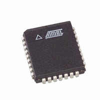
AT49LH00B4-33JC SL383 Atmel, AT49LH00B4-33JC SL383 Datasheet - Page 12

AT49LH00B4-33JC SL383
Manufacturer Part Number
AT49LH00B4-33JC SL383
Description
IC FLASH 4MBIT 33MHZ 32PLCC
Manufacturer
Atmel
Datasheet
1.AT49LH00B4-33JC.pdf
(41 pages)
Specifications of AT49LH00B4-33JC SL383
Format - Memory
FLASH
Memory Type
FLASH
Memory Size
4M (512K x 8)
Speed
33MHz
Interface
Parallel
Voltage - Supply
3 V ~ 3.6 V
Operating Temperature
0°C ~ 85°C
Package / Case
32-PLCC
Lead Free Status / RoHS Status
Contains lead / RoHS non-compliant
Figure 7-3.
Table 7-4.
Note:
12
Clock Cycle
FWH4/LFRAME
FWH/LAD[3:0]
3 - 9
10
11
12
13
14
15
16
17
2
1
1. Field contents are valid on the rising edge of the present clock cycle.
AT49LH00B4
CLK
FWH Write Cycle
FWH Write Cycle
Field Name
MADDR
RSYNC
START
MSIZE
IDSEL
DATA
DATA
TAR0
TAR1
TAR0
TAR1
1110b
START
1
IDSEL
IDSEL
2
0000b to 1111b
FWH/LAD[3:0]
0000b (ready)
A27-A24 A23-A20 A19-A16
Field Value
1111b (float)
1111b (float)
(indicates
1 byte)
1110b
0000b
1111b
1111b
YYYY
YYYY
YYYY
3
4
(1)
5
OUT then float
FWH/LAD[3:0
Float then IN
IN then float
A15-A12
] Direction
MADDR
Float then
OUT
OUT
6
IN
IN
IN
IN
IN
IN
A11-A8
7
A7-A4
Comments
FWH4/LFRAME must be active (low) for the device to respond.
Only the last START field (before FWH4/LFRAME transitioning
high) should be recognized. The START field contents indicate a
FWH memory write cycle.
Indicates which FWH memory device should respond. If the
IDSEL field matches the strapping values on ID[3:0], then that
particular device will respond to subsequent commands.
These seven clock cycles make up the 28-bit memory address.
YYYY is one nibble of the entire address. Addresses are
transferred with the most significant nibble first.
The MSIZE field indicates how many bytes will be transferred.
The device only supports single-byte operations, so MSIZE
must be 0000b.
YYYY is the least significant nibble of the data byte. The data
byte is either any valid Flash command or the data to be
programmed into the memory array.
YYYY is the most significant nibble of the data byte.
In this clock cycle, the master has driven the bus to all 1s and
then floats the bus prior to the next clock cycle. This is the first
part of the bus “turn-around cycle”.
The device takes control of the bus during this clock cycle.
During this clock cycle, the device will generate a “ready” SYNC
indicating that the data byte has been received.
The FWH memory device drives the bus to 1111b to indicate a
turn-around cycle.
The FWH memory device floats its outputs, and the master
regains control of the bus during this clock cycle.
8
A3-A0
9
0000b
MSIZE
10
D3-D0
DATA
11
D7-D4
DATA
12
1111b
TAR0
13
High-Z
TAR1
14
RSYNC
0000b
15
3379C–FLASH–3/05
1111b
TAR0
16
High-Z
TAR1
17


