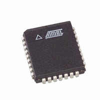
AT49LH00B4-33JC SL383 Atmel, AT49LH00B4-33JC SL383 Datasheet - Page 13

AT49LH00B4-33JC SL383
Manufacturer Part Number
AT49LH00B4-33JC SL383
Description
IC FLASH 4MBIT 33MHZ 32PLCC
Manufacturer
Atmel
Datasheet
1.AT49LH00B4-33JC.pdf
(41 pages)
Specifications of AT49LH00B4-33JC SL383
Format - Memory
FLASH
Memory Type
FLASH
Memory Size
4M (512K x 8)
Speed
33MHz
Interface
Parallel
Voltage - Supply
3 V ~ 3.6 V
Operating Temperature
0°C ~ 85°C
Package / Case
32-PLCC
Lead Free Status / RoHS Status
Contains lead / RoHS non-compliant
7.6
7.6.1
7.6.2
7.6.3
3379C–FLASH–3/05
LPC Memory Cycles
Start Field
CYCTYPE + DIR (Cycle Type And Direction) Field
MADDR (Memory Address) Field
A valid LPC memory cycle begins with the host driving the FWH4/LFRAME signal low for one or
more clock cycles. While the FWH4/LFRAME signal is low, a valid START value of 0000b must
be driven on the FWH/LAD[3:0] pins. Following the START field, a CYCTYPE + DIR (Cycle Type
and Direction) field must be sent to the device to indicate the type of cycle (e.g., memory access,
I/O access, etc.) and the direction (read or write) of the transfer. After the CYCTYPE + DIR field
has been sent, the 8-clock MADDR (Memory Address) field must be sent to the device to pro-
vide the 32-bit starting address location of where to begin reading or writing in the memory.
Figure 7-4.
This 1-clock field indicates the start of a cycle. It is valid on the last clock that FWH4/LFRAME is
sampled low. The start field that is used for an LPC cycle is 0000b. If the start field that is sam-
pled is not 0000b, then the cycle attempted is not an LPC memory cycle. It may be a valid FWH
memory cycle that the device will attempt to decode.
This 1-clock field is used to indicate the type of cycle and the direction of the transfer to be per-
formed. Of the four bits placed on the FWH/LAD[3:0] pins, bits[3:2] must be 01b to indicate that
the transfer will be a memory cycle. Values other than 01b, which may be used to specify an I/O
cycle or a DMA cycle for other components in the system, will cause the device to enter standby
mode when the FWH4/LFRAME pin is brought high and no internal operation is in progress. The
FWH/LAD[3:0] pins will also be placed in a high-impedance state.
Bit[1] is used to determine the direction of the transfer. 0 is used to indicate a read, and 1 is used
to indicate a write. Bit[0] is ignored and reserved for future use.
CYCTYPE + DIR fields that the device will respond to.
Table 7-5.
This is an 8-clock field that is used to provide a 32-bit (A31 - A0) memory address. The 32
address bits allow for the provisioning to access up to 4 GB of memory space.
The AT49LH00B4 only decodes the last six MADDR nibbles (A23 - A0) and ignores address bits
A31 - A24. Address bit A23 is used to determine whether reads or writes to the device will be
directed to the memory array (A23 = 1) or to the register space (A23 = 0).
Unlike FWH memory cycles, LPC cycles do not use an IDSEL field to determine which LPC
device in the system is being selected. Instead, the strapping values on the ID[3:0] pins are
compared against address bits A22 - A19 in the MADDR field. For the actual comparison, the
FWH/LAD[3:0]
010xb
011xb
FWH4/LFRAME
FWH/LAD[3:0]
CLK
LPC Memory Cycle Initiation and Addressing
Valid CYCTYPE + DIR Values
Cycle Type
LPC Memory Read
LPC Memory Write
START
CYCTYPE
+ DIR
MADDR MADDR MADDR
MADDR
MADDR MADDR MADDR MADDR
Table 7-5
AT49LH00B4
details the two valid
13


