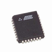
AT49LH00B4-33JC SL383 Atmel, AT49LH00B4-33JC SL383 Datasheet - Page 28

AT49LH00B4-33JC SL383
Manufacturer Part Number
AT49LH00B4-33JC SL383
Description
IC FLASH 4MBIT 33MHZ 32PLCC
Manufacturer
Atmel
Datasheet
1.AT49LH00B4-33JC.pdf
(41 pages)
Specifications of AT49LH00B4-33JC SL383
Format - Memory
FLASH
Memory Type
FLASH
Memory Size
4M (512K x 8)
Speed
33MHz
Interface
Parallel
Voltage - Supply
3 V ~ 3.6 V
Operating Temperature
0°C ~ 85°C
Package / Case
32-PLCC
Lead Free Status / RoHS Status
Contains lead / RoHS non-compliant
16.3
16.4
16.4.1
28
Byte Program
Read Status Register
AT49LH00B4
Clear Status Register
actions. After a sector erase, the CUI remains in the Read Status Register mode until a new
command is issued.
Successful sector erase requires that the corresponding sector’s Write-Lock bit be cleared and
the corresponding hardware write protect pin (TBL or WP) be inactive. If using the Uniform Sec-
tor Erase command to erase all of the sub-sectors, then all of the sub-sectors must have their
Write-Lock bits cleared and the WP pin must be inactive. If a sector erase is attempted when the
sector is locked, the sector erase will fail, and the reason for the failure will be indicated in the
Status Register.
The erased state of the memory bits is a logical “1” (erased state of a byte is FFH).
The device is programmed on a byte-by-byte basis. The Byte Program command requires two
command cycles with the programming address and data being input on the second command
cycle. The device will automatically generate the required internal programming pulses, and all
programming operations are completely self-timed. Please note that the byte location being pro-
grammed must have already been erased to FFH. A “0” cannot be programmed back to a “1”;
only an erase operation can convert “0”s to “1”s.
After the Byte Program command is written, the device’s Status Register may be checked to
determine the WSM status and the result of the program operation. If a program error is
detected, the Status Register should be cleared before any corrective action is taken by the sys-
tem software. After a byte program operation, the CUI remains in the Read Status Register
mode until a new command is issued.
A successful program operation also requires that the corresponding sector’s Write-Lock bit be
cleared, and the corresponding hardware write protect pin (TBL or WP) be inactive. If a program
operation is attempted when the sector is locked, the operation will fail, and the reason for the
failure will be indicated in the Status Register.
The Status Register (SR) may be read to determine when a sector erase or program operation
completes and whether the operation completed successfully. The Status Register may be read
at any time by writing the Read Status Register command. After writing the Read Status Regis-
ter command, all subsequent read operations will return data from the Status Register until
another valid command is written to the device.
Error flags (SR[5,4,1]) in the Status Register can only be set to “1”s by the WSM and can only be
reset by the Clear Status Register command. Therefore, if an error is detected, the Status Reg-
ister must be cleared before beginning another operation to avoid ambiguity.
3379C–FLASH–3/05


