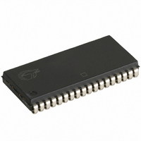
CY7C1049BV33-20VC Cypress Semiconductor Corp, CY7C1049BV33-20VC Datasheet

CY7C1049BV33-20VC
Specifications of CY7C1049BV33-20VC
Related parts for CY7C1049BV33-20VC
CY7C1049BV33-20VC Summary of contents
Page 1
... The eight input/output pins (I/O high-impedance state when the device is deselected (CE HIGH), the outputs are disabled (OE HIGH), or during a write operation (CE LOW, and WE LOW). The CY7C1049BV33 is available in a standard 400-mil-wide 36-pin SOJ and 44-pin TSOPII packages with center power and ground (revolutionary) pinout. A ...
Page 2
... Ind’ > > < MAX , Com’l/Ind’l CC – 0.3V, CC Com’l L > V – 0.3V < 0.3V CY7C1049BV33 [1] –0. 0.5V CC Ambient [2] Temperature 3.3V ± 0.3V 0°C to +70°C –40°C to +85°C -12 -15 -17 Max. Min. Max. Min. 2.4 2.4 0.4 0.4 V 2.2 V 2.2 ...
Page 3
... CC Com’ > V – 0.3V < 0.3V Test Conditions T = 25° MHz 3.3V CC VENIN EQUIVALENT 3.3V 167Ω 1.73V (b) GND RiseTime:1 V/ns CY7C1049BV33 -20 -25 Min. Max. Min. Max. 2.4 2.4 0.4 0.4 2 0 –0.5 0.8 –0.5 0.8 –1 +1 –1 +1 – ...
Page 4
... The input data set-up and hold timing should be referenced to the leading edge of the signal that terminates the write. 9. The minimum write cycle time for Write Cycle No. 3 (WE controlled, OE LOW) is the sum of t Document #: 38-05139 Rev. ** [4] Over the Operating Range -12 Min. Max. [ less than less than t HZCE LZCE HZOE LZOE CY7C1049BV33 -15 -17 Min. Max. Min. Max ...
Page 5
... No input may exceed V + 0.5V CC 11. .t < for the -12 and -15 speeds. t < for the -20 ns and slower speeds Document #: 38-05139 Rev. ** [4] Over the Operating Range (continued) Description [6] Over the Operating Range (For L version only) Description Conditions > > CY7C1049BV33 -20 -25 Min. Max. Min. Max ...
Page 6
... WE is HIGH for read cycle. 14. Address valid prior to or coincident with CE transition LOW. Document #: 38-05139 Rev. ** DATA RETENTION MODE 3.0V V > CDR OHA ACE t DOE t LZOE 50 CY7C1049BV33 3. DATA VALID t HZOE t HZCE IMPEDANCE DATA VALID t PD 50% 1049BV33-5 1049BV33–6 HIGH 1049BV33–7 Page ...
Page 7
... During this period the I/Os are in the output state and input signals should not be applied. Document #: 38-05139 Rev. ** [15, 16 SCE PWE t SD DATA [16 SCE PWE t HZWE – I/O Mode 0 7 Power-Down Read Write Selected, Outputs Disabled CY7C1049BV33 VALID DATA VALID t LZWE Power Standby (I SB Active ( Active ( Active ( 1049BV33–8 1049BV33-9 ) Page ...
Page 8
... CY7C1049BV33-12ZC CY7C1049BV33L-12VC CY7C1049BV33-12VI 15 CY7C1049BV33-15VC CY7C1049BV33L-15VC CY7C1049BV33-15ZC CY7C1049BV33L-15ZC CY7C1049BV33-15VI CY7C1049BV33-15ZI 17 CY7C1049BV33-17VC CY7C1049BV33L-17VC CY7C1049BV33-17ZC CY7C1049BV33L-17ZC CY7C1049BV33-17VI CY7C1049BV33L-17VI CY7C1049BV33-17ZI 20 CY7C1049BV33-20VC CY7C1049BV33L-20VC CY7C1049BV33-20ZC CY7C1049BV33L-20ZC CY7C1049BV33-20VI CY7C1049BV33-20ZI 25 CY7C1049BV33-25VC CY7C1049BV33L-25VC CY7C1049BV33-25ZC CY7C1049BV33L-25ZC CY7C1049BV33-25VI Document #: 38-05139 Rev. ** Package Name Package Type V36 36-Lead (400-Mil) Molded SOJ Z44 44-Pin TSOP II Z44 ...
Page 9
... The inclusion of Cypress Semiconductor products in life-support systems application implies that the manufacturer assumes all risk of such use and in doing so indemnifies Cypress Semiconductor against all charges. 36-Lead (400-Mil) Molded SOJ V36 44-Pin TSOP II Z44 CY7C1049BV33 51-85090-B 51-85087-A Page ...
Page 10
... Document Title: CY7C1049BV33 512K x 8 Static RAM Document Number: 38-05139 Issue REV. ECN NO. Date ** 113091 02/13/02 Document #: 38-05139 Rev. ** Orig. of Change DSG Change from Spec number: 38-00931 to 38-05139 CY7C1049BV33 Description of Change Page ...


