LNK614PG Power Integrations, LNK614PG Datasheet - Page 4
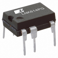
LNK614PG
Manufacturer Part Number
LNK614PG
Description
IC OFFLINE SWIT OTP CV/CC 8DIP
Manufacturer
Power Integrations
Series
LinkSwitch®-IIr
Type
Off Line Switcherr
Datasheet
1.LNK603DG.pdf
(18 pages)
Specifications of LNK614PG
Mfg Application Notes
LinkSwitch-II Family, Appl Note AN-44
Output Isolation
Isolated
Frequency Range
58 ~ 72kHz
Voltage - Output
700V
Power (watts)
4.1W
Operating Temperature
-40°C ~ 150°C
Package / Case
8-DIP (0.300", 7.62mm), 7 Leads
Output Voltage
700 V
Input / Supply Voltage (max)
9 V
Input / Supply Voltage (min)
- 0.3 V
Duty Cycle (max)
55 %
Switching Frequency
65 KHz
Supply Current
440 uA
Operating Temperature Range
- 40 C to + 150 C
Mounting Style
Through Hole
Maximum Operating Temperature
+ 150 C
Minimum Operating Temperature
- 40 C
Output Current
400 mA
Output Power
4.1 W
For Use With
596-1235 - KIT REF DESIGN LINKSWITCH 2
Lead Free Status / RoHS Status
Lead free / RoHS Compliant
Other names
596-1225-5
Available stocks
Company
Part Number
Manufacturer
Quantity
Price
Company:

Part Number:
LNK614PG
Manufacturer:
POWER
Quantity:
15 000
Part Number:
LNK614PG
Manufacturer:
POWER
Quantity:
20 000


Applications Example
Figure 4.
Circuit Description
This circuit shown in Figure 4 is configured as a primary-side
regulated flyback power supply utilizing the LNK613DG. With
an average efficiency of 74% and <30 mW no-load input power
this design easily exceeds the most stringent current energy
efficiency requirements.
Input Filter
AC input power is rectified by diodes D1 through D4. The
rectified DC is filtered by the bulk storage capacitors C1 and
C2. Inductor L1, C1 and C2 form a pi (π) filter, which attenuates
conducted differential-mode EMI noise. This configuration
along with Power Integrations transformer E-shield
allow this design to meet EMI standard EN55022 class B with
good margin without requiring a Y capacitor, even with the
output connected to safety earth ground. Fusible resistor RF1
provides protection against catastrophic failure. This should be
suitably rated (typically a wire wound type) to withstand the
instantaneous dissipation while the input capacitors charge
when first connected to the AC line.
LNK 613 Primary
The LNK613DG device (U1) incorporates the power switching
device, oscillator, CC/CV control engine, startup, and protection
functions. The integrated 700 V MOSFET provides a large drain
voltage margin in universal input AC applications, increasing
reliability and also reducing the output diode voltage stress by
allowing a greater transformer turns ratio. The device is
completely self-powered from the BYPASS pin and decoupling
capacitor C4. For the LNK61X devices, the bypass capacitor
value also selects the amount of output cable voltage drop
Rev. F 01/10
4
LNK603-606/613-616
Energy Efficient USB Charger Power Supply (74% Average Efficiency, <30 mW No-load Input Power).
Input
AC
8.2 Ω
2 W
RF1
1N4007
1N4007
D1
D3
1N4007
1N4007
D2
D4
4.7 µF
1.5 mH
400 V
C1
L1
470 kΩ
™
4.7 µF
400 V
R2
C2
technology
1N4007
300 Ω
D5
R3
LinkSwitch-II
820 pF
LNK613DG
25 V
1 µF
1 kV
C4
compensation. A 1 mF value selects the standard compensation.
A 10 mF value selects the enhanced compensation. Table 2
shows the amount of compensation for each device and
bypass capacitor value. The LNK60x devices do not provide
cable drop compensation.
The optional bias supply formed by D6 and C5 provides the
operating current for U1 via resistor R4. This reduces the
no-load consumption from ~200 mW to <30 mW and also
increases light load efficiency.
The rectified and filtered input voltage is applied to one side of
the primary winding of T1. The other side of the transformer’s
primary winding is driven by the integrated MOSFET in U1. The
leakage inductance drain voltage spike is limited by an RCD-R
clamp consisting of D5, R2, R3, and C3.
Output Rectification
The secondary of the transformer is rectified by D7, a 1 A, 40 V
Schottky barrier type for higher efficiency, and filtered by C7. If
lower efficiency is acceptable then this can be replaced with a
1 A PN junction diode for lower cost. In this application C7 was
sized to meet the required output voltage ripple specification
without requiring a post LC filter. To meet battery self discharge
requirement the pre-load resistor has been replaced with a
series resistor and Zener network (R8 and VR1). However in
designs where this is not a requirement a standard 1 kW
resistor can be used.
Output Regulation
The LNK613 regulates the output using ON/OFF control in the
constant voltage (CV) regulation region of the output character-
C3
U1
5
3
6.2 kΩ
R4
EE16
T1
LL4148
10 µF
16 V
D6
C5
10
NC
8
1
2
4
100 V
1 nF
C6
SS14
D7
8.87 kΩ
13 kΩ
200 Ω
1%
R5
1%
R7
R6
680 µF
10 V
C7
PI-5111-050808
2MM5230B-7
4.7 V
VR1
200 Ω
R8
www.powerint.com
5 V, 555 mA
Output
DC
Related parts for LNK614PG
Image
Part Number
Description
Manufacturer
Datasheet
Request
R

Part Number:
Description:
SOP-16
Manufacturer:
Power Integrations
Datasheet:
Part Number:
Description:
DIP8
Manufacturer:
Power Integrations
Datasheet:
Part Number:
Description:
TO-263
Manufacturer:
Power Integrations
Datasheet:
Part Number:
Description:
TO-263
Manufacturer:
Power Integrations
Datasheet:
Part Number:
Description:
Manufacturer:
Power Integrations
Datasheet: