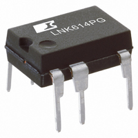
LNK614PG Power Integrations, LNK614PG Datasheet - Page 5

LNK614PG
Manufacturer Part Number
LNK614PG
Description
IC OFFLINE SWIT OTP CV/CC 8DIP
Manufacturer
Power Integrations
Series
LinkSwitch®-IIr
Type
Off Line Switcherr
Datasheet
1.LNK603DG.pdf
(18 pages)
Specifications of LNK614PG
Mfg Application Notes
LinkSwitch-II Family, Appl Note AN-44
Output Isolation
Isolated
Frequency Range
58 ~ 72kHz
Voltage - Output
700V
Power (watts)
4.1W
Operating Temperature
-40°C ~ 150°C
Package / Case
8-DIP (0.300", 7.62mm), 7 Leads
Output Voltage
700 V
Input / Supply Voltage (max)
9 V
Input / Supply Voltage (min)
- 0.3 V
Duty Cycle (max)
55 %
Switching Frequency
65 KHz
Supply Current
440 uA
Operating Temperature Range
- 40 C to + 150 C
Mounting Style
Through Hole
Maximum Operating Temperature
+ 150 C
Minimum Operating Temperature
- 40 C
Output Current
400 mA
Output Power
4.1 W
For Use With
596-1235 - KIT REF DESIGN LINKSWITCH 2
Lead Free Status / RoHS Status
Lead free / RoHS Compliant
Other names
596-1225-5
Available stocks
Company
Part Number
Manufacturer
Quantity
Price
Company:
Part Number:
LNK614PG
Manufacturer:
POWER
Quantity:
15 000
Part Number:
LNK614PG
Manufacturer:
POWER
Quantity:
20 000
istic and frequency control for constant current (CC) regulation.
The feedback resistors (R5 and R6) were selected using
standard 1% resistor values to center both the nominal output
voltage and constant current regulation thresholds.
Key Application Considerations
Output Power Table
The data sheet maximum output power table (Table 1) repre-
sents the maximum practical continuous output power level
that can be obtained under the following assumed conditions:
1. The minimum DC input voltage is 90 V or higher at 85 VAC
2. Secondary output of 5 V with a Schottky rectifier diode.
3. Assumed efficiency of 70%.
4. Discontinuous mode operation (K
5. The part is board mounted with SOURCE pins soldered to a
6. Ambient temperature of 50 °C for open frame designs and
Note: Higher output power are achievable if an output CC
tolerance >±10% is acceptable, allowing the device to be
operated at a higher SOURCE pin temperature.
Output Tolerance
LinkSwitch-II provides an overall output tolerance (including line,
component variation and temperature) of ±5% for the output
voltage in CV operation and ±10% for the output current during
CC operation over a junction temperature range of 0 °C to 100 °C
for the P/G package. For the D package (SO8) additional CC
variance may occur due to stress caused by the manufacturing
flow (i.e. solder-wave immersion or IR reflow). A sample power
supply build is recommended to verify production tolerances for
each design.
BYPASS Pin Capacitor Selection
For LinkSwitch-II 60x Family of Devices (without output
cable voltage drop compensation)
A 1 mF BYPASS pin capacitor is recommended. The capacitor
voltage rating should be greater than 7 V. The capacitor’s
dielectric material is not important but tolerance of capacitor
should be ≤ ±50%. The capacitor must be physically located
close to the LinkSwitch-II BYPASS pin.
For LinkSwitch-II 61x Family of Devices (with output cable
voltage drop compensation)
The amount of output cable compensation can be selected with
the value of the BYPASS pin capacitor. A value of 1 mF selects
the standard cable compensation. A 10 mF capacitor selects
the enhanced cable compensation. Table 2 shows the amount
of compensation for each LinkSwitch-II device and capacitor
value. The capacitor can be either ceramic or electrolytic but
tolerance and temperature variation should be ≤ ±50%.
www.powerint.com
input. The value of the input capacitance should be large
enough to meet these criteria for AC input designs.
sufficient area of copper to keep the SOURCE pin tempera-
ture at or below 90 °C.
an internal enclosure temperature of 60 °C for adapter
designs.
P
>1.3).
LinkSwitch-II Output Cable Voltage Drop Compensation
The output voltage that is entered into PIXls design spreadsheet
is the voltage at the end of the output cable when the power
supply is delivering maximum power. The output voltage at the
terminals of the supply is the value measured at the end of the
cable multiplied by the output voltage change factor.
LinkSwitch-II Layout Considerations
Circuit Board Layout
LinkSwitch-II is a highly integrated power supply solution that
integrates on a single die, both, the controller and the high
voltage MOSFET. The presence of high switching currents and
voltages together with analog signals makes it especially
important to follow good PCB design practice to ensure stable
and trouble free operation of the power supply. See Figure 5 for
a recommended circuit board layout for LinkSwitch-II.
When designing a printed circuit board for the LinkSwitch-II
based power supply, it is important to follow the following
guidelines:
Single Point Grounding
Use a single point (Kelvin) connection at the negative terminal of
the input filter capacitor for the LinkSwitch-II SOURCE pin and
bias winding return. This improves surge capabilities by
returning surge currents from the bias winding directly to the
input filter capacitor.
Bypass Capacitor
The BYPASS pin capacitor should be located as close as
possible to the SOURCE and BYPASS pins.
Feedback Resistors
Place the feedback resistors directly at the FEEDBACK pin of
the LinkSwitch-II device. This minimizes noise coupling.
Thermal Considerations
The copper area connected to the SOURCE pins provides the
LinkSwitch-II heat sink. A good estimate is that the LinkSwitch-II
will dissipate 10% of the output power. Provide enough copper
area to keep the SOURCE pin temperature below 90 °C. Higher
temperatures are allowable only if an output current (CC)
tolerance above ±10% is acceptable. In this case a maximum
SOURCE pin temperature below 110 °C is recommended to
provide margin for part to part R
Table 2.
LNK613
LNK614
LNK615
LNK616
Device
Capacitor Value.
Cable Compensation Change Factor vs Device and BYPASS Pin
Capacitor Value
BYPASS Pin
LNK603-606/613-616
10 mF
10 mF
10 mF
10 mF
1 mF
1 mF
1 mF
1 mF
DS(ON)
variation.
Output Voltage
Change Factor
1.035
1.055
1.045
1.065
1.050
1.070
1.060
1.090
Rev. F 01/10
5


