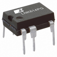
LNK614PG Power Integrations, LNK614PG Datasheet - Page 7

LNK614PG
Manufacturer Part Number
LNK614PG
Description
IC OFFLINE SWIT OTP CV/CC 8DIP
Manufacturer
Power Integrations
Series
LinkSwitch®-IIr
Type
Off Line Switcherr
Datasheet
1.LNK603DG.pdf
(18 pages)
Specifications of LNK614PG
Mfg Application Notes
LinkSwitch-II Family, Appl Note AN-44
Output Isolation
Isolated
Frequency Range
58 ~ 72kHz
Voltage - Output
700V
Power (watts)
4.1W
Operating Temperature
-40°C ~ 150°C
Package / Case
8-DIP (0.300", 7.62mm), 7 Leads
Output Voltage
700 V
Input / Supply Voltage (max)
9 V
Input / Supply Voltage (min)
- 0.3 V
Duty Cycle (max)
55 %
Switching Frequency
65 KHz
Supply Current
440 uA
Operating Temperature Range
- 40 C to + 150 C
Mounting Style
Through Hole
Maximum Operating Temperature
+ 150 C
Minimum Operating Temperature
- 40 C
Output Current
400 mA
Output Power
4.1 W
For Use With
596-1235 - KIT REF DESIGN LINKSWITCH 2
Lead Free Status / RoHS Status
Lead free / RoHS Compliant
Other names
596-1225-5
Available stocks
Company
Part Number
Manufacturer
Quantity
Price
Company:
Part Number:
LNK614PG
Manufacturer:
POWER
Quantity:
15 000
Part Number:
LNK614PG
Manufacturer:
POWER
Quantity:
20 000
Figure 8.
BYPASS pin voltage. The parameters I
the parameter table of the LinkSwitch-II data sheet. Diode D6 can
be any low cost diode such as FR102, 1N4148 or BAV19/20/21.
Quick Design Checklist
As with any power supply design, all LinkSwitch-II designs
should be verified on the bench to make sure that component
specifications are not exceeded under worst-case conditions.
The following minimum set of tests is strongly recommended:
1. Maximum drain voltage – Verify that peak V
2. Maximum drain current – At maximum ambient temperature,
www.powerint.com
680 V at the highest input voltage and maximum output power.
maximum input voltage and maximum output load, verify
drain current waveforms at start-up for any signs of trans-
Figure 6.
LinkSwitch-II Flyback Power Supply Without Bias Supply.
Input
Desired Drain Voltage Waveform with Minimal Leakage
Ringing Undershoot.
AC
8.2 Ω
2 W
RF1
1N4007
1N4007
D1
D3
1N4007
1N4007
An overshoot
is acceptable
D2
D4
S2
and V
4.7 µF
400 V
1 mH
DS
C1
L1
BP
does not exceed
are provided in
470 kΩ
4.7 µF
400 V
R2
C2
1N4007
300 Ω
D5
R3
3. Thermal check – At maximum output power, both minimum
Design Tools
Up-to-date information on design tools can be found at the
Power Integrations web site: www.powerint.com
LinkSwitch-II
820 pF
LNK613DG
50 V
1 kV
1 µF
former saturation and excessive leading edge current spikes.
LinkSwitch-II has a leading edge blanking time of 170 ns to
prevent premature termination of the ON-cycle.
and maximum input voltage and maximum ambient tempera-
ture; verify that temperature specifications are not exceeded
for LinkSwitch-II, transformer, output diodes and output
capacitors. Enough thermal margin should be allowed for
part-to-part variation of the R
in the data sheet. To assure 10% CC tolerance a maximum
SOURCE pin temperature of 90 ºC is recommended.
C4
C3
Figure 7.
U1
5
3
EE13
Ring Undershoot.
TI
Undesirable Drain Voltage Waveform with Large Leakage
10
NC
8
2
4
SL13
D7
9.31 kΩ
13 kΩ
LNK603-606/613-616
1%
R5
1%
R6
470 µF
10 V
C7
DS(ON)
PI-5116-050808
of LinkSwitch-II, as specified
1 kΩ
Negative ring may
increase output
ripple and/or
degrade output
regulation
Output
DC
Rev. F 01/10
7


