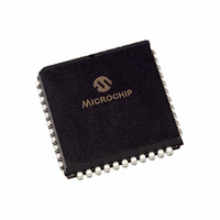
TC820CLW Microchip Technology, TC820CLW Datasheet - Page 9

TC820CLW
Manufacturer Part Number
TC820CLW
Description
IC ADC 3 3/4DGT LGC PROBE 44PLCC
Manufacturer
Microchip Technology
Datasheet
1.TC820CPL.pdf
(34 pages)
Specifications of TC820CLW
Display Type
LCD
Configuration
7 Segment + 2 Annunciators
Digits Or Characters
A/D 3.75 Digits
Current - Supply
1mA
Voltage - Supply
9V
Operating Temperature
0°C ~ 70°C
Mounting Type
Surface Mount
Package / Case
44-PLCC
Lead Free Status / RoHS Status
Lead free / RoHS Compliant
Interface
-
Available stocks
Company
Part Number
Manufacturer
Quantity
Price
Company:
Part Number:
TC820CLW
Manufacturer:
Microchip Technology
Quantity:
10 000
Company:
Part Number:
TC820CLW713
Manufacturer:
Microchip Technology
Quantity:
10 000
In a simple dual slope converter, a complete conver-
sion requires the integrator output to "ramp-up" from
zero and "ramp-down" back to zero. A simple mathe-
matical equation relates the input signal, reference
voltage, and integration time.
EQUATION 3-1:
For a constant V
EQUATION 3-2:
FIGURE 3-1:
Accuracy in a dual slope converter is unrelated to the
integrating resistor and capacitor values as long as
they are stable during a measurement cycle. An
inherent benefit of the dual slope technique is noise
immunity. Noise spikes are integrated or averaged to
zero during the integration periods, making integrating
ADCs immune to the large conversion errors that
plague successive approximation converters in high
noise environments. Interfering signals, with frequency
components at multiples of the averaging (integrating)
period, will be attenuated
ADCs commonly operate with the signal integration
period set to a multiple of the 50/60Hz power line
period.
© 2007 Microchip Technology Inc.
Where: V
Integrate Time
Fixed Signal
Input Signal
Analog
Voltage
REF
R
t
t
INT
INT
DEINT
REF
1
C
INT
INT
R
= Reference Voltage
= Integration Time
= De-integration Time
Polarity Control
V
∫
:
Variable Reference
Integrate Time
IN
t
0
INT
Display
Switch
Driver
= V
Integrator
Basic Dual Slope Converter.
V
–
+
IN
REF
C
V
V
(t)dt =
IN
IN
Phase
Control
(Figure
= V
= 1.2V
t
DEINT
t
INT
REF
V
–
+
Comparator
R
REF
REF
INT
Control
Logioc
3-2). Integrating
t
C
DEINT
INT
Counter
Clock
FIGURE 3-2:
Dual Slope Converter.
3.2
In addition to the basic integrate and de-integrate dual
slope phases discussed above, the TC820 design
incorporates a "zero integrator output" phase and an
"auto-zero" phase. These additional phases ensure
that the integrator starts at 0V (even after a severe over
range conversion), and that all offset voltage errors
(buffer amplifier, integrator and comparator) are
removed from the conversion. A true digital zero
reading is assured without any external adjustments.
A complete conversion consists of four distinct phases:
1.
2.
3.
4.
3.2.1
This phase guarantees that the integrator output is at
0V before the system zero phase is entered, ensuring
that the true system offset voltages will be compen-
sated for even after an over range conversion. The
duration of this phase is 500 counts plus the unused
de-integrate counts.
3.2.2
During the auto-zero phase, the differential input signal
is disconnected from the measurement circuit by
opening internal analog switches, and the internal
nodes are shorted to Analog Common (0V
establish a zero input condition. Additional analog
switches close a feedback loop around the integrator
and comparator to permit comparator offset voltage
error compensation. A voltage established on C
compensates for internal device offset voltages during
the measurement cycle. The auto-zero phase residual
is typically 10 µV to 15 mV. The auto-zero duration is
1500 counts.
Zero Integrator Output.
Auto-Zero.
Signal Integrate.
Reference De-integrate.
30
20
10
0.1/T
0
T = Measurement
Analog Section
ZERO INTEGRATOR OUTPUT
PHASE
AUTO-ZERO PHASE
Period
Input Frequency
Normal Mode Rejection of
1/T
DS21476C-page 9
TC820
REF
AZ
10/T
then
) to


