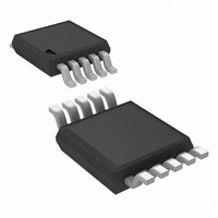
LM5067MM-2/NOPB National Semiconductor, LM5067MM-2/NOPB Datasheet - Page 4

LM5067MM-2/NOPB
Manufacturer Part Number
LM5067MM-2/NOPB
Description
IC CTLR NEG HOTSWAP A/R 10MSOP
Manufacturer
National Semiconductor
Type
Hot-Swap Controllerr
Datasheet
1.LM5067MM-1NOPB.pdf
(24 pages)
Specifications of LM5067MM-2/NOPB
Applications
General Purpose
Internal Switch(s)
No
Voltage - Supply
-9 V ~ -80 V
Operating Temperature
-40°C ~ 125°C
Mounting Type
Surface Mount
Package / Case
10-TFSOP, 10-MSOP (0.118", 3.00mm Width)
For Use With
LM5067EVAL - NEGATIVE HOT SWAP / INRUSH CURRE
Lead Free Status / RoHS Status
Lead free / RoHS Compliant
Other names
LM5067MM-2TR
Available stocks
Company
Part Number
Manufacturer
Quantity
Price
Company:
Part Number:
LM5067MM-2/NOPB
Manufacturer:
TI
Quantity:
4 500
www.national.com
Input
OUT Pin
SENSE Pin
UVLO, OVLO Pins
Gate Control (GATE Pin)
Current into VCC (100 µs pulse)
OUT, PGD to VEE
UVLO, OVLO to VEE
SENSE to VEE
ESD Rating
Human Body Model
Absolute Maximum Ratings
If Military/Aerospace specified devices are required,
please contact the National Semiconductor Sales Office/
Distributors for availability and specifications.
Electrical Characteristics
junction temperature (T
correlation. Typical values represent the most likely parametric norm at T
Unless otherwise stated the following conditions apply: I
VEE. See
POR
OVLO
UVLO
OVLO
UVLO
UVLO
OVLO
UVLO
OVLO
Symbol
POR
I
I
I
I
I
POR
OUT-DIS
SNS-DIS
V
I
OUT-EN
SNS-EN
CC-DIS
I
CC-EN
GATE
GATE
V
EN-HYS
Z
BIAS
BIAS
EN
HYS
DEL
HYS
DEL
IT
TH
TH
(Note
(Note
3).
2)
Parameter
Operating voltage, VCC – VEE
Internal operating current, enabled
Internal operating current, disabled
Threshold voltage to start insertion timer
Threshold voltage to enable all functions
POR
OUT bias current, enabled
OUT bias current, disabled
SENSE bias current, enabled
SENSE bias current, disabled
UVLO threshold
UVLO hysteresis current
UVLO delay
UVLO bias current
OVLO threshold
OVLO hysteresis current
OVLO delay
OVLO bias current
Source current
Sink current
Gate output voltage in normal operation
J
) range of -40°C to +125°C. Minimum and Maximum limits are guaranteed through test, design, or statistical
EN
hysteresis
Limits in standard type are for T
-0.3V to +0.3V
-0.3V to 100V
(Note
-0.3V to 17V
100 mA
1)
CC
2kV
= 2 mA, OUT Pin = 48V above VEE, all voltages are with respect to
4
Storage Temperature
Junction Temperature
Conditions
I
VCC-VEE = 11V,
UVLO = 5V
VCC-VEE = 11V,
UVLO = 2V
VCC-VEE increasing
VCC-VEE increasing
VCC-VEE decreasing
OUT = VEE, Normal operation
Disabled, OUT = VEE + 48V
OUT = VEE, Normal operation
Disabled, OUT = VEE + 48V
UVLO = VEE + 2V
Delay to GATE high
Delay to GATE low
UVLO = VEE + 5V
OVLO = VEE+2.8V
Delay to GATE high
Delay to GATE low
OVLO = VEE + 2.4V
Normal Operation
UVLO < 2.5V
SENSE - VEE =150 mV or
VCC - VEE < POR
GATE-VEE voltage
Operating Ratings
Current into VCC
OUT Voltage above VEE
PGD Off Voltage above VEE
Junction Temperature
CC
= 2 mA, UVLO = 5V
J
= 25°C, and are provided for reference purposes only.
J
= 25°C only; limits in boldface type apply over the
(Note
IT
, V
GATE
5)
= 5V
12.35
2.45
2.43
Min
-34
-72
1.9
10
45
2 mA (min)
0V to 80V
0V to 80V
−40°C to +125°C
Typ
480
125
110
-50
-22
-52
0.8
7.7
8.4
0.1
2.5
2.5
2.2
13
50
22
26
12
26
12
V
-6
-65°C to +150°C
Z
13.65
Max
2.55
2.57
2.68
660
200
-10
-32
8.2
8.7
34
1
1
1
+150°C
Units
mA
mV
mA
µA
µA
µA
µA
µA
µA
µA
µA
µs
µs
µs
µs
V
V
V
V
V
V


