BD6067GU-E2 Rohm Semiconductor, BD6067GU-E2 Datasheet - Page 12
BD6067GU-E2
Manufacturer Part Number
BD6067GU-E2
Description
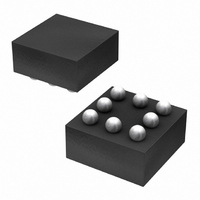
IC LED DRIVR WHITE BCKLGT 8-VCSP
Manufacturer
Rohm Semiconductor
Type
Backlight, White LEDr
Specifications of BD6067GU-E2
Topology
PWM, Step-Up (Boost)
Number Of Outputs
1
Internal Driver
Yes
Type - Primary
Backlight
Type - Secondary
White LED
Frequency
800kHz ~ 1.2MHz
Voltage - Supply
2.7 V ~ 5.5 V
Voltage - Output
30V
Mounting Type
Surface Mount
Package / Case
8-VCSP
Operating Temperature
-30°C ~ 85°C
Current - Output / Channel
30mA
Internal Switch(s)
Yes
Led Driver Application
Mobile Phones
No. Of Outputs
1
Output Current
30mA
Output Voltage
36V
Input Voltage
2.7V To 5.5V
Operating Temperature Range
-30°C To +85°C
Driver
RoHS Compliant
Lead Free Status / RoHS Status
Lead free / RoHS Compliant
Efficiency
-
Lead Free Status / Rohs Status
Details
Other names
BD6067GU-E2TR
Available stocks
Company
Part Number
Manufacturer
Quantity
Price
Company:

Part Number:
BD6067GU-E2
Manufacturer:
RICOH
Quantity:
3 000
Part Number:
BD6067GU-E2
Manufacturer:
ROHM/罗姆
Quantity:
20 000


© 2011 ROHM Co., Ltd. All rights reserved.
BD6067GU, BD6069GUT, BD6071HFN, BD6072HFN
►BD6071HFN
●Block diagram, recommended circuit example, pin location diagram
●Pin assignment table
●Operation
www.rohm.com
BD6071HFN is a fixed frequency PWM current mode DC/DC converter, and adopts synchronous rectification architecture.
As for the inputs of the PWM comparator as the feature of the PWM current mode, one is overlapped with error components
from the error amplifier, and the other is overlapped with a current sense signal that controls the inductor current into Slope
waveform for sub harmonic oscillation prevention. This output controls Q1 and Q2 via the RS latch.
Timing of Q1 and Q2 is precisely adjusted so that they will not turn ON at the same time, thus putting them into
non-overlapped relation.
In the period where Q1 is ON, energy is accumulated in the external inductor, and in the period where Q1 is OFF, energy is
transferred to the capacitor of VOUT via Q2.
Further, BD6071HFN has many safety functions, and their detection signals stop switching operation at once.
PIN Name
GNDA
VOUT
TEST
GND
VFB
VIN
SW
EN
1μF
C
In/Out
Out
IN
In
In
In
In
In
-
-
VIN
Q1
GND
SW
22μH
Pin number
L
Fig.34 Block diagram and recommended circuit diagram
Q2
GNDA
1
2
3
8
4
7
6
5
Fig.35 Pin location diagram HSON8 (Top view)
Q
Q
Current
Sence
S
R
300kΩ
Analog GND
Power supply input
Feedback input voltage
Enable control(pull down is integrated on resistance)
TEST input (pull down is integrated on resistance)
Output
Switching terminal
Power GND
8
1
TSD
Control
EN
7
2
12/29
3
6
TEST
4
5
PWMcomp
over voltage
short protect
protect
-
+
OSC
+
Function
ERRAMP
+
-
+
-
-
+
V
VOUT
FB
C
1μF
OUT
24Ω
R
FB
white LED
2011.01 - Rev.C
Technical Note
Related parts for BD6067GU-E2
Image
Part Number
Description
Manufacturer
Datasheet
Request
R

Part Number:
Description:
Multifunction LED Display Panel
Manufacturer:
CARLO GAVAZZI
Datasheet:

Part Number:
Description:
Manufacturer:
Rohm Semiconductor
Datasheet:
Part Number:
Description:
Manufacturer:
Rohm Semiconductor
Datasheet:
Part Number:
Description:
Manufacturer:
Rohm Semiconductor
Datasheet:
Part Number:
Description:
Manufacturer:
Rohm Semiconductor
Datasheet:
Part Number:
Description:
Manufacturer:
Rohm Semiconductor
Datasheet:
Part Number:
Description:
Manufacturer:
Rohm Semiconductor
Datasheet:
Part Number:
Description:
Manufacturer:
Rohm Semiconductor
Datasheet:
Part Number:
Description:
Manufacturer:
Rohm Semiconductor
Datasheet:
Part Number:
Description:
Manufacturer:
Rohm Semiconductor
Datasheet:
Part Number:
Description:
Manufacturer:
Rohm Semiconductor
Datasheet:
Part Number:
Description:
Manufacturer:
Rohm Semiconductor
Datasheet:
Part Number:
Description:
Manufacturer:
Rohm Semiconductor
Datasheet: