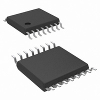
LM3421MH/NOPB National Semiconductor, LM3421MH/NOPB Datasheet - Page 15

LM3421MH/NOPB
Manufacturer Part Number
LM3421MH/NOPB
Description
IC LED DRVR HP CONS CURR 16TSSOP
Manufacturer
National Semiconductor
Series
PowerWise®r
Type
High Power, Constant Currentr
Datasheet
1.LM3421MHNOPB.pdf
(48 pages)
Specifications of LM3421MH/NOPB
Constant Current
Yes
Topology
PWM, SEPIC, Step-Down (Buck), Step-Up (Boost)
Number Of Outputs
1
Internal Driver
No
Type - Primary
Automotive
Type - Secondary
High Brightness LED (HBLED)
Frequency
2MHz
Voltage - Supply
4.5 V ~ 75 V
Voltage - Output
3 V ~ 72 V
Mounting Type
Surface Mount
Package / Case
16-TSSOP Exposed Pad, 16-eTSSOP, 16-HTSSOP
Operating Temperature
-40°C ~ 125°C
Current - Output / Channel
1A
Internal Switch(s)
No
Efficiency
95%
Lead Free Status / RoHS Status
Lead free / RoHS Compliant
Other names
*LM3421MH/NOPB
LM3421MH
LM3421MH
To mitigate this problem, a compensator should be designed
to give adequate phase margin (above 45°) at the crossover
frequency. A simple compensator using a single capacitor at
the COMP pin (C
which will ensure adequate phase margin if placed low
enough. At high duty cycles (as shown in
zero places extreme limits on the achievable bandwidth with
this type of compensation. However, because an LED driver
is essentially free of output transients (except catastrophic
failures open or short), the dominant pole approach, even with
reduced bandwidth, is usually the best approach. The domi-
nant compensation pole (ω
output resistance (R
It may also be necessary to add one final pole at least one
decade above the crossover frequency to attenuate switching
noise and, in some cases, provide better gain margin. This
pole can be placed across R
resistor at the same time.
sation is physically implemented in the system.
The high frequency pole (ω
The total system transfer function becomes:
The resulting compensated loop gain frequency response
shown in
phase margin (above 45°) if the dominant compensation pole
is placed low enough, ensuring stability:
FIGURE 10. Compensated Loop Gain Frequency
Figure 10
CMP
O
indicates that the system has adequate
) will add a dominant pole to the system,
) of the error amplifier (typically 5 MΩ):
Response
Figure 9
P2
P3
SNS
) is determined by C
) can be calculated:
to filter the ESL of the sense
shows how the compen-
Figure
8), the RHP
CMP
300673a4
and the
15
START-UP REGULATOR
The LM3421/23 includes a high voltage, low dropout bias
regulator. When power is applied, the regulator is enabled
and sources current into an external capacitor (C
nected to the V
for the V
V
protects the device from attempting to operate with insuffi-
cient supply voltage and the supply is also internally current
limited.
LM3421/23.
First, C
(~4.2V). The C
C
which can be estimated as:
Once C
the LED current is in regulation. The C
can be roughly estimated as:
The system start-up time (t
In some configurations, the start-up waveform will overshoot
the steady state COMP pin voltage. In this case, the LED cur-
rent and output voltage will overshoot also, which can trip the
over-voltage or protection, causing a race condition. The eas-
iest way to prevent this is to use a larger compensation
capacitor (C
CC
CMP
regulator is monitored by an internal UVLO circuit that
is then charged to 0.9V over the charging time (t
Figure 11
CMP
BYP
CC
= 0.9V, the part starts switching to charge C
regulator is 2.2 µF to 3.3 µF. The output of the
is charged to be above V
CMP
FIGURE 11. Start-Up Waveforms
CC
VCC
), thereby slowing down the control loop.
pin. The recommended bypass capacitance
shows the typical start-up waveforms for the
charging time (t
SU
) is defined as:
VCC
) can be estimated as:
O
CC
charging time (t
UVLO threshold
30067361
www.national.com
BYP
) con-
O
CMP
until
CO
)
)


