MAX16823ATE+ Maxim Integrated Products, MAX16823ATE+ Datasheet - Page 2
MAX16823ATE+
Manufacturer Part Number
MAX16823ATE+
Description
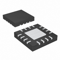
IC LED DRIVR HIGH BRIGHT 16-TQFN
Manufacturer
Maxim Integrated Products
Type
HBLED Driverr
Datasheet
1.MAX16823ATE.pdf
(12 pages)
Specifications of MAX16823ATE+
Constant Current
Yes
Topology
Linear (LDO), Open Drain, PWM
Number Of Outputs
3
Internal Driver
Yes
Type - Primary
Automotive
Type - Secondary
High Brightness LED (HBLED), RGB
Voltage - Supply
5.5 V ~ 40 V
Voltage - Output
3.41V
Mounting Type
Surface Mount
Package / Case
16-TQFN Exposed Pad
Operating Temperature
-40°C ~ 125°C
Current - Output / Channel
100mA
Internal Switch(s)
Yes
Operating Supply Voltage
5.5 V to 40 V
Maximum Power Dissipation
2666 mW
Maximum Operating Temperature
+ 125 C
Mounting Style
SMD/SMT
Minimum Operating Temperature
- 40 C
Lead Free Status / RoHS Status
Lead free / RoHS Compliant
Frequency
-
Efficiency
-
Lead Free Status / Rohs Status
Lead free / RoHS Compliant


ABSOLUTE MAXIMUM RATINGS
High-Voltage, 3-Channel Linear High-Brightness
LED Driver with Open LED Detection
IN to GND ...............................................................-0.3V to +45V
OUT1, OUT2, OUT3, DIM1, DIM2,
REG, LGC, LEDGOOD to GND ................................-0.3V to +6V
CS1, CS2, CS3 to GND .........................................-0.3V to +0.5V
OUT1, OUT2, OUT3 Short Circuited
Maximum Current into Any Pin
Stresses beyond those listed under “Absolute Maximum Ratings” may cause permanent damage to the device. These are stress ratings only, and functional
operation of the device at these or any other conditions beyond those indicated in the operational sections of the specifications is not implied. Exposure to
absolute maximum rating conditions for extended periods may affect device reliability.
ELECTRICAL CHARACTERISTICS
(V
to +125°C, unless otherwise noted. Typical values are at T
2
Supply Voltage Range
Undervoltage Lockout
Ground Current
Guaranteed Output Current
LED Current-Sense Accuracy
Dropout Voltage (Note 2)
Output Current Slew Rate
Short-Circuit Current
LEDGOOD
LEDGOOD Output Logic Low
LGC Pullup Resistor
LGC Input Upper Threshold
LGC Input Lower Threshold
LGC Pulldown Current
LGC Clock Period
DIMMING INPUT (DIM1, DIM2, DIM3)
DIM_ Logic-Input Bias Current
DIM_ Input-Voltage High
DIM_ Input-Voltage Low
DIM_ Frequency
OUTPUTS (OUT1, OUT2, AND OUT3) (Note 3)
Turn-On Time
Turn-Off Time
Output Current Rise Time
Output Current Fall Time
IN
DIM3 to GND ...........................................-0.3V to (V
to GND Duration (V
(except IN, OUT1, OUT2, OUT3)..................................±20mA
_______________________________________________________________________________________
= 12V, C
PARAMETER
REG
= 0.1µF, I
IN
+ 16V) ..........................................60min
REG
= 0, C
SYMBOL
LGC
UVLO
ΔVDO
V
V
I
I
V
DIM_
V
OUT
UTH
I
LTH
OL
G
IN
= 15nF, V
V
V
I
5mA ≤ I
I
I
V
I
V
C
DIM_ rising edge to 90% of OUT_ current
DIM_ falling edge to 10% of OUT_ current
10% to 90%
90% to 10%
OUT1
OUT_
OUT_
SINK
IN
IN
OUT_
LGC
LGC
DIM1
IN
rising
falling
= 2mA
> V
= 70mA, 6.5V ≤ V
= 70mA, 5.5V ≤ V
= 15nF
= I
+ 0.3V)
= 0V
OUT_
A
= V
OUT2
UTH
= +25°C.) (Note 1)
DIM2
≤ 70mA
= I
CONDITIONS
OUT3
= V
Continuous Power Dissipation (T
Operating Temperature Range .........................-40°C to +125°C
Junction Temperature ......................................................+150°C
Storage Temperature Range .............................-65°C to +150°C
Lead Temperature (soldering, 10s) .................................+300°C
DIM3
16-Pin TQFN 5mm x 5mm
16-Pin TSSOP (derate 26.1mW/°C above +70°C) ....2088.8mW
= 70mA
IN
IN
(derate 33.3mW/°C above +70°C) .........................2666mW
≤ 40V
≤ 6.5V
= 3.4V, R
CS_
= 2.85Ω from CS_ to GND, T
MIN
0.77
-0.1
100
5.5
4.4
4.0
2.4
65
0
A
= +70°C)
TYP
2.53
180
100
4.9
4.6
1.5
0.3
0.3
0.8
1.5
20
12
8
8
7
6
MAX
+0.1
135
V
5.4
5.2
0.7
0.8
0.4
2.3
0.6
40
28
18
18
15
3
5
3
IN
J
= T
A
UNITS
mA/µs
= -40°C
kHz
mA
mA
mA
mA
ms
kΩ
µA
µs
µs
µs
µs
%
V
V
V
V
V
V
V
V
Related parts for MAX16823ATE+
Image
Part Number
Description
Manufacturer
Datasheet
Request
R

Part Number:
Description:
3-Channel Linear High-Brightness LED Driver
Manufacturer:
Maxim Integrated Products
Datasheet:

Part Number:
Description:
MAX7528KCWPMaxim Integrated Products [CMOS Dual 8-Bit Buffered Multiplying DACs]
Manufacturer:
Maxim Integrated Products
Datasheet:
Part Number:
Description:
Single +5V, fully integrated, 1.25Gbps laser diode driver.
Manufacturer:
Maxim Integrated Products
Datasheet:
Part Number:
Description:
Single +5V, fully integrated, 155Mbps laser diode driver.
Manufacturer:
Maxim Integrated Products
Datasheet:
Part Number:
Description:
VRD11/VRD10, K8 Rev F 2/3/4-Phase PWM Controllers with Integrated Dual MOSFET Drivers
Manufacturer:
Maxim Integrated Products
Datasheet:
Part Number:
Description:
Highly Integrated Level 2 SMBus Battery Chargers
Manufacturer:
Maxim Integrated Products
Datasheet:
Part Number:
Description:
Current Monitor and Accumulator with Integrated Sense Resistor; ; Temperature Range: -40°C to +85°C
Manufacturer:
Maxim Integrated Products
Part Number:
Description:
TSSOP 14/A°/RS-485 Transceivers with Integrated 100O/120O Termination Resis
Manufacturer:
Maxim Integrated Products
Part Number:
Description:
TSSOP 14/A°/RS-485 Transceivers with Integrated 100O/120O Termination Resis
Manufacturer:
Maxim Integrated Products
Part Number:
Description:
QFN 16/A°/AC-DC and DC-DC Peak-Current-Mode Converters with Integrated Step
Manufacturer:
Maxim Integrated Products
Part Number:
Description:
TDFN/A/65V, 1A, 600KHZ, SYNCHRONOUS STEP-DOWN REGULATOR WITH INTEGRATED SWI
Manufacturer:
Maxim Integrated Products
Part Number:
Description:
Integrated Temperature Controller f
Manufacturer:
Maxim Integrated Products
Part Number:
Description:
SOT23-6/I°/45MHz to 650MHz, Integrated IF VCOs with Differential Output
Manufacturer:
Maxim Integrated Products
Part Number:
Description:
SOT23-6/I°/45MHz to 650MHz, Integrated IF VCOs with Differential Output
Manufacturer:
Maxim Integrated Products