MAX16823ATE+ Maxim Integrated Products, MAX16823ATE+ Datasheet - Page 5
MAX16823ATE+
Manufacturer Part Number
MAX16823ATE+
Description
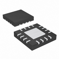
IC LED DRIVR HIGH BRIGHT 16-TQFN
Manufacturer
Maxim Integrated Products
Type
HBLED Driverr
Datasheet
1.MAX16823ATE.pdf
(12 pages)
Specifications of MAX16823ATE+
Constant Current
Yes
Topology
Linear (LDO), Open Drain, PWM
Number Of Outputs
3
Internal Driver
Yes
Type - Primary
Automotive
Type - Secondary
High Brightness LED (HBLED), RGB
Voltage - Supply
5.5 V ~ 40 V
Voltage - Output
3.41V
Mounting Type
Surface Mount
Package / Case
16-TQFN Exposed Pad
Operating Temperature
-40°C ~ 125°C
Current - Output / Channel
100mA
Internal Switch(s)
Yes
Operating Supply Voltage
5.5 V to 40 V
Maximum Power Dissipation
2666 mW
Maximum Operating Temperature
+ 125 C
Mounting Style
SMD/SMT
Minimum Operating Temperature
- 40 C
Lead Free Status / RoHS Status
Lead free / RoHS Compliant
Frequency
-
Efficiency
-
Lead Free Status / Rohs Status
Lead free / RoHS Compliant


High-Voltage, 3-Channel Linear High-Brightness
TQFN
5, 6, 7
10
11
12
13
14
15
16
—
1
2
3
4
8
9
PIN
TSSOP
7, 8, 9
10
11
12
13
14
15
16
—
3
4
5
6
1
2
_______________________________________________________________________________________
LEDGOOD
NAME
OUT3
OUT2
OUT1
DIM1
DIM2
DIM3
GND
LGC
REG
CS3
CS2
CS1
EP
IN
LED Driver with Open LED Detection
D i m m i ng Inp ut 1. D IM 1 i s a l ow - fr eq uency d i m m i ng i np ut for channel 1. A l og i c- l ow tur ns off
O U T1 and a l og i c- hi g h tur ns on O U T1.
D i m m i ng Inp ut 2. D IM 2 i s a l ow - fr eq uency d i m m i ng i np ut for channel 2. A l og i c- l ow tur ns off
O U T2 and a l og i c- hi g h tur ns on O U T2.
D i m m i ng Inp ut 3. D IM 3 i s a l ow - fr eq uency d i m m i ng i np ut for channel 3. A l og i c- l ow tur ns off
O U T3 and a l og i c- hi g h tur ns on O U T3.
Open LED Output. LEDGOOD is an open-drain output. A logic-high indicates the LED
connection i s g ood i n al l thr ee channel s. A l og i c- l ow i nd i cates an op en LE D connecti on. S ee the
LE D GO OD secti on.
P osi ti ve Inp ut S up p l y. Byp ass w i th a 0.1µF ( m i n) cap aci tor to G N D . C onnect al l IN
p i ns tog ether .
LE D D etecti on- Ti m i ng S etti ng . C onnect a cap aci tor fr om LGC to g r ound to set the d el ay ti m e
for LE D G OO D .
3.4V V ol tag e Reg ul ator . C onnect a 0.1µF cap aci tor fr om RE G to G N D .
G r ound
C hannel 3 S ense Am p l i fi er P osi ti ve Inp ut. C onnect the cur r ent- sense r esi stor b etw een C S 3
and G N D to p r og r am the outp ut cur r ent l evel for channel 3.
C hannel 2 S ense Am p l i fi er P osi ti ve Inp ut. C onnect the cur r ent- sense r esi stor b etw een C S 2
and G N D to p r og r am the outp ut cur r ent l evel for channel 2.
C hannel 1 S ense Am p l i fi er P osi ti ve Inp ut. C onnect the cur r ent- sense r esi stor b etw een C S 1
and G N D to p r og r am the outp ut cur r ent l evel for channel 1.
C ur r ent Reg ul ator O utp ut 3
C ur r ent Reg ul ator O utp ut 2
C ur r ent Reg ul ator O utp ut 1
E xp osed P ad . C onnect E P to a l ar g e- ar ea g r ound p l ane for effecti ve p ow er d i ssi p ati on. D o not
use as the IC g r ound connecti on.
FUNCTION
Pin Description
5
Related parts for MAX16823ATE+
Image
Part Number
Description
Manufacturer
Datasheet
Request
R

Part Number:
Description:
3-Channel Linear High-Brightness LED Driver
Manufacturer:
Maxim Integrated Products
Datasheet:

Part Number:
Description:
MAX7528KCWPMaxim Integrated Products [CMOS Dual 8-Bit Buffered Multiplying DACs]
Manufacturer:
Maxim Integrated Products
Datasheet:
Part Number:
Description:
Single +5V, fully integrated, 1.25Gbps laser diode driver.
Manufacturer:
Maxim Integrated Products
Datasheet:
Part Number:
Description:
Single +5V, fully integrated, 155Mbps laser diode driver.
Manufacturer:
Maxim Integrated Products
Datasheet:
Part Number:
Description:
VRD11/VRD10, K8 Rev F 2/3/4-Phase PWM Controllers with Integrated Dual MOSFET Drivers
Manufacturer:
Maxim Integrated Products
Datasheet:
Part Number:
Description:
Highly Integrated Level 2 SMBus Battery Chargers
Manufacturer:
Maxim Integrated Products
Datasheet:
Part Number:
Description:
Current Monitor and Accumulator with Integrated Sense Resistor; ; Temperature Range: -40°C to +85°C
Manufacturer:
Maxim Integrated Products
Part Number:
Description:
TSSOP 14/A°/RS-485 Transceivers with Integrated 100O/120O Termination Resis
Manufacturer:
Maxim Integrated Products
Part Number:
Description:
TSSOP 14/A°/RS-485 Transceivers with Integrated 100O/120O Termination Resis
Manufacturer:
Maxim Integrated Products
Part Number:
Description:
QFN 16/A°/AC-DC and DC-DC Peak-Current-Mode Converters with Integrated Step
Manufacturer:
Maxim Integrated Products
Part Number:
Description:
TDFN/A/65V, 1A, 600KHZ, SYNCHRONOUS STEP-DOWN REGULATOR WITH INTEGRATED SWI
Manufacturer:
Maxim Integrated Products
Part Number:
Description:
Integrated Temperature Controller f
Manufacturer:
Maxim Integrated Products
Part Number:
Description:
SOT23-6/I°/45MHz to 650MHz, Integrated IF VCOs with Differential Output
Manufacturer:
Maxim Integrated Products
Part Number:
Description:
SOT23-6/I°/45MHz to 650MHz, Integrated IF VCOs with Differential Output
Manufacturer:
Maxim Integrated Products