LP3936SLX/NOPB National Semiconductor, LP3936SLX/NOPB Datasheet - Page 10
LP3936SLX/NOPB
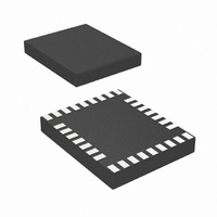
Manufacturer Part Number
LP3936SLX/NOPB
Description
IC LED DRVR WT/RGB BCKLGT 32TCSP
Manufacturer
National Semiconductor
Series
PowerWise®r
Type
Backlight, White LED, RGB (I²C Interface)r
Datasheet
1.LP3936SLNOPB.pdf
(21 pages)
Specifications of LP3936SLX/NOPB
Constant Current
Yes
Topology
PWM, Step-Up (Boost)
Number Of Outputs
9
Internal Driver
Yes
Type - Primary
Backlight, Flash/Torch, LED Blinker, Light Management Unit (LMU)
Type - Secondary
RGB, White LED
Frequency
1MHz
Voltage - Supply
3 V ~ 6 V
Voltage - Output
5.3V
Mounting Type
Surface Mount
Package / Case
32-Laminate TCSP
Operating Temperature
-40°C ~ 85°C
Current - Output / Channel
120mA
Internal Switch(s)
Yes
Efficiency
90%
Lead Free Status / RoHS Status
Lead free / RoHS Compliant
Other names
LP3936SLX


2
I
C Compatible Interface
(Continued)
2
I
C START AND STOP CONDITIONS
2
START and STOP bits classify the beginning and the end of the I
C session. START condition is defined as SDA signal
transitioning from HIGH to LOW while SCL line is HIGH. STOP condition is defined as the SDA transitioning from LOW to HIGH
2
2
while SCL is HIGH. The I
C master always generates START and STOP bits. The I
C bus is considered to be busy after START
2
condition and free after STOP condition. During data transmission, I
C master can generate repeated START conditions. First
START and repeated START conditions are equivalent, function-wise.
20081412
TRANSFERRING DATA
Every byte put on the SDA line must be eight bits long, with the most significant bit (MSB) being transferred first. Each byte of data
has to be followed by an acknowledge bit. The acknowledge related clock pulse is generated by the master. The transmitter
releases the SDA line (HIGH) during the acknowledge clock pulse. The receiver must pull down the SDA line during the 9th clock
pulse, signifying an acknowledge. A receiver which has been addressed must generate an acknowledge after each byte has been
received.
2
After the START condition, the I
C master sends a chip address. This address is seven bits long followed by an eighth bit which
is a data direction bit (R/W). The LP3936 address is 36h. For the eighth bit, a “0” indicates a WRITE and a “1” indicates a READ.
The second byte selects the register to which the data will be written. The third byte contains data to write to the selected register.
2
I
C Chip Address
20081413
2
I
C Write Cycle
20081414
w = write (SDA = “0”)
r = read (SDA = “1”)
ack = acknowledge (SDA pulled down by either master or slave)
rs = repeated start
id = chip address, 36h for LP3936
When a READ function is to be accomplished, a WRITE function must precede the READ function, as shown in the Read Cycle
waveform.
www.national.com
10
Related parts for LP3936SLX/NOPB
Image
Part Number
Description
Manufacturer
Datasheet
Request
R

Part Number:
Description:
Manufacturer:
National Semiconductor
Datasheet:
Part Number:
Description:
Manufacturer:
National Semiconductor
Datasheet:

Part Number:
Description:
IC LED DRVR WT/RGB BCKLGT 32TCSP
Manufacturer:
National Semiconductor
Datasheet:
Part Number:
Description:
National Semiconductor [8-Bit D/A Converter]
Manufacturer:
National Semiconductor
Datasheet:
Part Number:
Description:
National Semiconductor [Media Coprocessor]
Manufacturer:
National Semiconductor
Datasheet:
Part Number:
Description:
Digitally Controlled Tone and Volume Circuit with Stereo Audio Power Amplifier, Microphone Preamp Stage and National 3D Sound
Manufacturer:
National Semiconductor
Datasheet:
Part Number:
Description:
Digitally Controlled Tone and Volume Circuit with Stereo Audio Power Amplifier, Microphone Preamp Stage and National 3D Sound
Manufacturer:
National Semiconductor
Datasheet:
Part Number:
Description:
AC97 Rev 2 Codec with Sample Rate Conversion and National 3D Sound
Manufacturer:
National Semiconductor
Part Number:
Description:
Manufacturer:
National Semiconductor
Datasheet:
Part Number:
Description:
Manufacturer:
National Semiconductor
Datasheet:
Part Number:
Description:
General Purpose, Low Voltage, Low Power, Rail-to-Rail Output Operational Amplifiers
Manufacturer:
National Semiconductor
Datasheet:
Part Number:
Description:
8-bit 20 MSPS flash A/D converter.
Manufacturer:
National Semiconductor
Datasheet:
Part Number:
Description:
Low Noise Quad Operational Amplifier
Manufacturer:
National Semiconductor
Datasheet:
Part Number:
Description:
Quad Differential Line Receivers
Manufacturer:
National Semiconductor
Datasheet: