LP3936SLX/NOPB National Semiconductor, LP3936SLX/NOPB Datasheet - Page 14
LP3936SLX/NOPB
Manufacturer Part Number
LP3936SLX/NOPB
Description
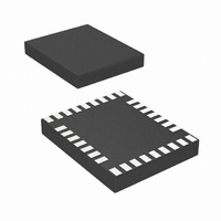
IC LED DRVR WT/RGB BCKLGT 32TCSP
Manufacturer
National Semiconductor
Series
PowerWise®r
Type
Backlight, White LED, RGB (I²C Interface)r
Datasheet
1.LP3936SLNOPB.pdf
(21 pages)
Specifications of LP3936SLX/NOPB
Constant Current
Yes
Topology
PWM, Step-Up (Boost)
Number Of Outputs
9
Internal Driver
Yes
Type - Primary
Backlight, Flash/Torch, LED Blinker, Light Management Unit (LMU)
Type - Secondary
RGB, White LED
Frequency
1MHz
Voltage - Supply
3 V ~ 6 V
Voltage - Output
5.3V
Mounting Type
Surface Mount
Package / Case
32-Laminate TCSP
Operating Temperature
-40°C ~ 85°C
Current - Output / Channel
120mA
Internal Switch(s)
Yes
Efficiency
90%
Lead Free Status / RoHS Status
Lead free / RoHS Compliant
Other names
LP3936SLX


www.national.com
I
V
RDS
f
t
I
Symbol
LOAD
PWF
STARTUP
CL_OUT
OUT
Magnetic Boost DC/DC Converter Electrical Characteristics
PFM/PWM Mode
User can change the Boost converters mode between PWM (Pulse Width Modulation) and PFM (Pulse Frequency Modulation).
The startup is done on PFM mode and then the device runs on PWM mode (as a default). User can set PFM mode by turning
“pfm_mode” register bit HIGH. PFM is recommended to use with light loads and PWM with high loads.
Boost Standby Mode
User can set boost converter to STANDBY mode by writing register bit EN_BOOST low. This mode can be useful when driving
LEDs directly from battery voltage. This may be possible if LED forward voltage is low, battery voltage is high and LED current
is low.
When EN_BOOST is written high, the converter starts for 10 ms in PFM mode and then goes to PWM mode if PWM mode has
been selected (default). During Boost Start-up all LEDs are turned off to reduce the load.
Unused Boost Converter
If the boost converter is not used, it should be disabled by writing bit en_boost low. OUT pin should be connected to GND and
FB pin to the LED supply voltage.
Boost Converter Typical Performance Characteristics
otherwise stated.
ON
Load Current
Output Voltage Accuracy (FB Pin)
Output Voltage (FB Pin)
Switch ON Resistance
PWM Mode Switching Frequency
Frequency Accuracy
Startup Time
OUT Pin Current Limit
Boost Converter Efficiency
Parameter
3.0V ≤ V
V
1 mA ≤ I
3.0V ≤ V
V
1 mA ≤ I
3.0V
V
1 mA ≤ I
V
V
RT = 82 kΩ
RT = 82 kΩ
V
OUT
OUT
(SCHOTTKY)
IN
DD1,2
DD
20081419
>
= 3.6V
<
= 4.55V
= 4.55V
4.55V + V
= 3.6V, I
V
LOAD
LOAD
LOAD
IN
IN
IN
≤ 4.5V
≤ V (FB)−0.5V
Conditions
<
≤ 225 mA
≤ 250 mA
≤ 250 mA
4.55V +
SW
14
(SCHOTTKY)
= 0.5A
Boost Frequency vs RT Resistor
Min
−10
600
400
−5
−6
0
V
V
IN
IN
= 3.6V, V
–V
(SCHOTTKY)
4.55
Typ
750
0.4
±
25
1
3
OUT
= 4.55V if not
1050
1200
Max
250
+10
0.5
+5
+6
20081420
Units
MHz
mA
mA
ms
%
%
Ω
V
V
Related parts for LP3936SLX/NOPB
Image
Part Number
Description
Manufacturer
Datasheet
Request
R

Part Number:
Description:
Manufacturer:
National Semiconductor
Datasheet:
Part Number:
Description:
Manufacturer:
National Semiconductor
Datasheet:

Part Number:
Description:
IC LED DRVR WT/RGB BCKLGT 32TCSP
Manufacturer:
National Semiconductor
Datasheet:
Part Number:
Description:
National Semiconductor [8-Bit D/A Converter]
Manufacturer:
National Semiconductor
Datasheet:
Part Number:
Description:
National Semiconductor [Media Coprocessor]
Manufacturer:
National Semiconductor
Datasheet:
Part Number:
Description:
Digitally Controlled Tone and Volume Circuit with Stereo Audio Power Amplifier, Microphone Preamp Stage and National 3D Sound
Manufacturer:
National Semiconductor
Datasheet:
Part Number:
Description:
Digitally Controlled Tone and Volume Circuit with Stereo Audio Power Amplifier, Microphone Preamp Stage and National 3D Sound
Manufacturer:
National Semiconductor
Datasheet:
Part Number:
Description:
AC97 Rev 2 Codec with Sample Rate Conversion and National 3D Sound
Manufacturer:
National Semiconductor
Part Number:
Description:
Manufacturer:
National Semiconductor
Datasheet:
Part Number:
Description:
Manufacturer:
National Semiconductor
Datasheet:
Part Number:
Description:
General Purpose, Low Voltage, Low Power, Rail-to-Rail Output Operational Amplifiers
Manufacturer:
National Semiconductor
Datasheet:
Part Number:
Description:
8-bit 20 MSPS flash A/D converter.
Manufacturer:
National Semiconductor
Datasheet:
Part Number:
Description:
Low Noise Quad Operational Amplifier
Manufacturer:
National Semiconductor
Datasheet:
Part Number:
Description:
Quad Differential Line Receivers
Manufacturer:
National Semiconductor
Datasheet: