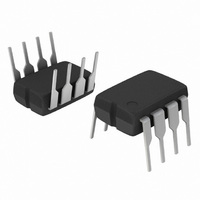
MC33151PG ON Semiconductor, MC33151PG Datasheet - Page 3

MC33151PG
Manufacturer Part Number
MC33151PG
Description
IC MOSFET DRIVER DUAL HS 8-DIP
Manufacturer
ON Semiconductor
Type
High Speedr
Datasheet
1.MC33151PG.pdf
(12 pages)
Specifications of MC33151PG
Configuration
Low-Side
Input Type
Inverting
Delay Time
35ns
Current - Peak
1.5A
Number Of Configurations
2
Number Of Outputs
2
Voltage - Supply
6.5 V ~ 18 V
Operating Temperature
-40°C ~ 125°C
Mounting Type
Through Hole
Package / Case
8-DIP (0.300", 7.62mm)
Rise Time
31 ns
Fall Time
32 ns
Supply Voltage (min)
6.5 V
Supply Current
10.5 mA
Maximum Power Dissipation
1000 mW
Maximum Operating Temperature
+ 85 C
Mounting Style
Through Hole
Minimum Operating Temperature
- 40 C
Number Of Drivers
2
Driver Configuration
Inverting
Driver Type
High Speed
Input Logic Level
CMOS/LSTTL
Propagation Delay Time
100ns
Operating Supply Voltage (max)
18V
Peak Output Current
1.5A
Power Dissipation
1W
Operating Supply Voltage (min)
6.5V
Operating Supply Voltage (typ)
12V
Turn Off Delay Time
100fs
Turn On Delay Time (max)
100ps
Operating Temp Range
-40C to 85C
Operating Temperature Classification
Industrial
Mounting
Through Hole
Pin Count
8
Package Type
PDIP
Lead Free Status / RoHS Status
Lead free / RoHS Compliant
High Side Voltage - Max (bootstrap)
-
Lead Free Status / Rohs Status
Lead free / RoHS Compliant
Other names
MC33151PG
MC33151PGOS
MC33151PGOS
Available stocks
Company
Part Number
Manufacturer
Quantity
Price
Company:
Part Number:
MC33151PG
Manufacturer:
TOSHIBA
Quantity:
32 000
Part Number:
MC33151PG
Manufacturer:
ON/安森美
Quantity:
20 000
1. For optimum switching speed, the maximum input voltage should be limited to 10 V or V
2. Maximum package power dissipation limits must be observed.
3. T
ELECTRICAL CHARACTERISTICS
ambient temperature range that applies [Note 3], unless otherwise noted.)
LOGIC INPUTS
DRIVE OUTPUT
SWITCHING CHARACTERISTICS (T
TOTAL DEVICE
Input Threshold Voltage −
Input Current − High State (V
Input Current
Output Voltage − Low State (I
Output Voltage − Low State
Output Voltage − Low State
Output Voltage
Output Voltage − High State
Output Voltage − High State
Output Pulldown Resistor
Propagation Delay (10% Input to 10% Output, C
Drive Output Rise Time (10% to 90%) C
Drive Output Rise Time (10% to 90%)
Drive Output Fall Time (90% to 10%) C
Drive Output Fall Time (90% to 10%)
Power Supply Current
Operating Voltage
Logic Input to Drive Output Rise
Logic Input to Drive Output Fall
Standby (Logic Inputs Grounded)
Operating (C
low
= 0°C for MC34151
−40°C for MC33151
− Low State (V
L
− High State (I
= 1.0 nF Drive Outputs 1 and 2, f = 100 kHz)
IL
(I
(I
(I
(I
IH
Source
Source
Source
Sink
Sink
Sink
= 0.8 V)
= 2.6 V)
= 10 mA)
= 50 mA)
= 400 mA)
Characteristics
= 10 mA)
= 50 mA)
= 400 mA)
A
C
= 25°C)
C
L
L
Output Transition Low to High State
Output Transition High to Low State
L
L
= 1.0 nF
= 2.5 nF
(V
T
= 1.0 nF
= 2.5 nF
high
CC
= 12 V, for typical values T
L
= +70°C for MC34151
= 1.0 nF)
+85°C for MC33151
http://onsemi.com
3
A
= 25°C, for min/max values T
CC
t
t
PLH(in/out)
PHL(in/out)
, whichever is less.
Symbol
V
V
R
V
V
I
V
I
I
CC
OH
t
IH
IL
OL
PD
t
CC
IH
IL
r
f
A
10.5
10.4
Min
0.8
9.5
6.5
is the only operating
−
−
−
−
−
−
−
−
−
−
−
−
−
−
−
1.75
1.58
10.9
10.5
11.2
11.1
Typ
200
100
0.8
1.1
1.7
6.0
20
35
36
14
31
16
32
−
Max
500
100
100
100
2.6
1.2
1.5
2.5
30
30
10
15
18
−
−
−
−
−
−
−
Unit
mA
kW
mA
ns
ns
ns
V
V
V


