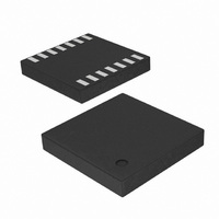
SI8235BB-C-IMR Silicon Laboratories Inc, SI8235BB-C-IMR Datasheet - Page 26

SI8235BB-C-IMR
Manufacturer Part Number
SI8235BB-C-IMR
Description
IC ISODRIVER DUAL LOW SIDE 14LGA
Manufacturer
Silicon Laboratories Inc
Datasheet
1.SI8234BB-C-IS1.pdf
(52 pages)
Specifications of SI8235BB-C-IMR
Configuration
Low-Side
Input Type
Non-Inverting
Delay Time
60ns
Current - Peak
4A
Number Of Configurations
2
Number Of Outputs
2
Voltage - Supply
6.5 V ~ 24 V
Operating Temperature
-40°C ~ 125°C
Mounting Type
Surface Mount
Package / Case
14-LGA
Lead Free Status / RoHS Status
Lead free / RoHS Compliant
High Side Voltage - Max (bootstrap)
-
Si823x
3.7.4. Control Inputs
VIA, VIB, and PWM inputs are high-true, TTL level-compatible logic inputs. A logic high signal on VIA or VIB
causes the corresponding output to go high. For PWM input versions (Si8231/4), VOA is high and VOB is low when
the PWM input is high, and VOA is low and VOB is high when the PWM input is low.
3.7.5. Disable Input
When brought high, the DISABLE input unconditionally drives VOA and VOB low regardless of the states of VIA
and VIB. Device operation terminates within tSD after DISABLE = V
DISABLE = V
3.8. Programmable Dead Time and Overlap Protection
All high-side/low-side drivers (Si8230/1/3/4) include programmable overlap protection to prevent outputs VOA and
VOB from being high at the same time. These devices also include programmable dead time, which adds a user-
programmable delay between transitions of VOA and VOB (Figure 26.A). When enabled, dead time is present on
all transitions, even after overlap recovery (Figure 26.B). The amount of dead time delay (DT) is programmed by a
single resistor (RDT) connected from the DT input to ground per Equation 5. Note that the dead time pin can be
tied to VDDI or left floating to provide a nominal dead time at approximately 400 ps.
The device driving VIA and VIB should provide a minimum dead time of TDD to avoid activating overlap protection.
Input/output timing waveforms for the two-input drivers are shown in Figure 40, and dead time waveforms are
shown in Figure 41.
26
PWM
VIA/
VOA
VOB
VIB
Figure 40. Input / Output Waveforms for High-Side / Low-Side Two-Input Drivers
IL
A
. The DISABLE input has no effect if VDDI is below its UVLO level (i.e. VOA, VOB remain low).
B
C
D
E
DT 10 RDT
where:
DT
and
RDT
F
=
G H
=
dead time (ns)
dead time programming resistor (k
I
Equation 5.
Rev. 1.1
Ref
A
B
C
D
E
G
H
F
I
Normal operation: VIA high, VIB low.
Normal operation: VIB high, VIA low.
Contention: VIA = VIB = high.
Recovery from contention: VIA transitions low.
Normal operation: VIA = VIB = low.
Normal operation: VIA high, VIB low.
Contention: VIA = VIB = high.
Recovery from contention: VIB transitions low.
Normal operation: VIB transitions high.
IH
and resumes within tRESTART after
Description


