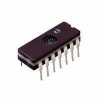
TC4467MJD Microchip Technology, TC4467MJD Datasheet - Page 3

TC4467MJD
Manufacturer Part Number
TC4467MJD
Description
IC MOSFET DVR QUAD NAND 14CDIP
Manufacturer
Microchip Technology
Type
Microcontrollerr
Datasheet
1.TC4469CPD.pdf
(22 pages)
Specifications of TC4467MJD
Configuration
Low-Side
Input Type
NAND
Delay Time
40ns
Current - Peak
1.2A
Number Of Configurations
4
Number Of Outputs
4
Voltage - Supply
4.5 V ~ 18 V
Operating Temperature
-55°C ~ 125°C
Mounting Type
Through Hole
Package / Case
14-CDIP (0.300", 7.62mm)
Rise Time
25 ns
Fall Time
25 ns
Supply Voltage (min)
4.5 V
Supply Current
4 mA
Maximum Power Dissipation
840 mW
Maximum Operating Temperature
+ 125 C
Mounting Style
Through Hole
Minimum Operating Temperature
- 55 C
Number Of Drivers
4
Lead Free Status / RoHS Status
Lead free / RoHS Compliant
High Side Voltage - Max (bootstrap)
-
Lead Free Status / Rohs Status
Lead free / RoHS Compliant
Available stocks
Company
Part Number
Manufacturer
Quantity
Price
Company:
Part Number:
TC4467MJD
Manufacturer:
VISHAY
Quantity:
6 000
1.0
Absolute Maximum Ratings†
Supply Voltage ...............................................................+20 V
Input Voltage ............................. (GND – 5 V) to (V
Package Power Dissipation: (T
Package Thermal Resistance:
Operating Temperature Range:
Maximum Chip Temperature ....................................... +150°C
Storage Temperature Range.........................-65°C to +150°C
ELECTRICAL SPECIFICATIONS
Electrical Characteristics: Unless otherwise noted, T
Input
Logic 1, High Input Voltage
Logic 0, Low Input Voltage
Input Current
Output
High Output Voltage
Low Output Voltage
Output Resistance
Peak Output Current
Continuous Output Current
Latch-Up Protection Withstand
Reverse Current
Switching Time (Note 1)
Rise Time
Fall Time
Delay Time
Delay Time
Power Supply
Power Supply Current
Power Supply Voltage
Note
2002 Microchip Technology Inc.
PDIP...................................................................800 mW
CERDIP .............................................................840 mW
SOIC ..................................................................760 mW
CERDIP R
CERDIP R
PDIP R
PDIP R
SOIC R
SOIC R
C Version ................................................... 0°C to +70°C
E Version.................................................-40°C to +85°C
M Version ..............................................-55°C to +125°C
1:
2:
3:
ELECTRICAL
CHARACTERISTICS
Totem pole outputs should not be paralleled because the propagation delay differences from one to the other could cause one driver to
drive high a few nanoseconds before another. The resulting current spike, although short, may decrease the life of the device. Switching
times are ensured by design.
When driving all four outputs simultaneously in the same direction, V
will cause high-power dissipation in the device.
The input threshold has approximately 50 mV of hysteresis centered at approximately 1.5 V. Input rise times should be kept below 5 µsec
to avoid high internal peak currents during input transitions. Static input levels should also be maintained above the maximum, or below
the minimum, input levels specified in the "Electrical Characteristics" to avoid increased power dissipation in the device.
Parameters
J-A
J-C
J-A
J-C
J-A
J-C
..........................................................80°C/W
..........................................................35°C/W
..........................................................95°C/W
..........................................................28°C/W
...................................................100°C/W
.....................................................23°C/W
A
70°C)
Sym
V
V
V
V
V
R
I
I
t
t
I
PK
DC
t
t
D1
D2
I
IN
OH
DD
OL
IH
I
R
F
S
IL
O
V
DD
DD
+ 0.3 V)
Min
-1.0
2.4
– 0.025
4.5
—
—
—
—
—
—
—
—
—
—
—
—
A
= +25°C, with 4.5 V
TC4467/TC4468/TC4469
Typ
500
1.2
1.5
—
—
—
—
—
10
—
—
15
15
40
40
—
†Notice: Stresses above those listed under "Maximum
Ratings" may cause permanent damage to the device. This is
a stress rating only and functional operation of the device at
those or any other conditions above those indicated in the
operation listings of this specification is not implied. Exposure
to maximum rating conditions for extended periods may affect
device reliability.
DD
will be limited to 16 V. This reduces the chance that internal dv/dt
Max
V
+1.0
0.15
300
500
0.8
15
25
25
75
75
18
—
—
—
DD
4
V
DD
Units
nsec
nsec
nsec
nsec
mA
mA
mA
µA
V
V
V
V
A
V
18 V.
Note 3
Note 3
0 V
I
I
I
Single Output
Total Package
4.5 V
Figure 4-1
Figure 4-1
Figure 4-1
Figure 4-1
Note 2
LOAD
LOAD
OUT
= 10 mA, V
V
= 100 µA (Note 1)
= 10 mA (Note 1)
IN
V
DD
V
DD
Conditions
16 V
DD
= 18 V
DS21425B-page 3


