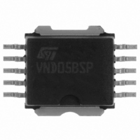
VND05BSP13TR STMicroelectronics, VND05BSP13TR Datasheet

VND05BSP13TR
Specifications of VND05BSP13TR
Available stocks
Related parts for VND05BSP13TR
VND05BSP13TR Summary of contents
Page 1
... Built-in thermal shutdown protects the chip from over temperature and short circuit. The status output provides an indication of open load in on state, open load in off state, overtemperature conditions and stuck- Tube VND05BSP Rev 3 VND05BSP 10 1 PowerSO-10 Order codes Tape & reel VND05BSP13TR . CC 1/16 www.st.com 16 ...
Page 2
Contents Contents 1 Block diagram and pin description . . . . . . . . . . . . . . . . . . . . . . . . . . . . . 5 2 Electrical ...
Page 3
VND05BSP List of tables Table 1. Device summary . . . . . . . . . . . . . . . . . . . . . . . . . . . . . . . . ...
Page 4
List of figures List of figures Figure 1. Block diagram . . . . . . . . . . . . . . . . . . . . . . . . . . . . . . ...
Page 5
VND05BSP 1 Block diagram and pin description Figure 1. Block diagram Figure 2. Configuration diagram (top view) Block diagram and pin description 5/16 ...
Page 6
... These are stress ratings only and operation of the device at these or any other conditions above those indicated in the operating sections of this specification is not implied. Exposure to Absolute maximum rating conditions for extended periods may affect device reliability. Refer also to the STMicroelectronics sure program and other relevant quality document. Table 2. ...
Page 7
VND05BSP 2.2 Thermal data Table 3. Thermal data Symbol R Thermal resistance junction-case thj-case R Thermal resistance junction-ambient thj-amb 2.3 Electrical characteristics Values specified in this section are for 8<V stated. Table 4. Power Symbol V Supply voltage CC (1) ...
Page 8
Electrical specifications Table 6. Logic inputs Symbol V Input low level voltage IL (1) V Input high level voltage IH V Input hysteresis voltage I(hyst.) I Input current IN V Input clamp voltage ICL 1. The V is internally clamped ...
Page 9
VND05BSP Figure 4. I L(off) Figure pol Figure 6. Switching time waveforms circuit waveforms povl Electrical specifications 9/16 ...
Page 10
Electrical specifications Table 8. Truth table Conditions Normal operation Undervoltage Thermal shutdown Openload Output shorted to V Figure 7. Waveforms 10/16 Input 1 Input Channel 1 H Channel Channel Channel ...
Page 11
VND05BSP 3 Application information Figure 8. Typical application circuit with a schottky diode for reverse supply protection Figure 9. Typical application circuit with separate signal ground Application information 11/16 ...
Page 12
Application information 3.1 Functional description The device has a diagnostic output which indicates open load in on-state, open load in off- state, over temperature conditions and stuck- From the falling edge of the input signal, the status output, ...
Page 13
VND05BSP 4 Package and packing information ® 4.1 ECOPACK In order to meet environmental requirements, ST offers these devices in ECOPACK packages. ECOPACK is marked on the package and on the inner box label, in compliance with JEDEC Standard JESD97. ...
Page 14
Package and packing information Table 9. PowerSO-10 mechanical data Dim (1) L ...
Page 15
VND05BSP 5 Revision history Table 10. Document revision history Date Apr-2001 03-May-2006 24-Nov-2008 Revision 1 Initial release. Added contents, list of tables and figures. 2 Added Table 10.: Document revision Document reformatted and restructured. 3 Added Table 1.: Device Added ...
Page 16
... Information in this document is provided solely in connection with ST products. STMicroelectronics NV and its subsidiaries (“ST”) reserve the right to make changes, corrections, modifications or improvements, to this document, and the products and services described herein at any time, without notice. All ST products are sold pursuant to ST’s terms and conditions of sale. ...


