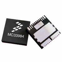
MC33984BPNAR2 Freescale Semiconductor, MC33984BPNAR2 Datasheet - Page 20

MC33984BPNAR2
Manufacturer Part Number
MC33984BPNAR2
Description
IC SWITCH HI SIDE DUAL 16-PQFN
Manufacturer
Freescale Semiconductor
Type
High Sider
Datasheet
1.MC33984BPNAR2.pdf
(38 pages)
Specifications of MC33984BPNAR2
Input Type
SPI
Number Of Outputs
2
On-state Resistance
4 mOhm
Voltage - Supply
6 V ~ 27 V
Operating Temperature
-40°C ~ 125°C
Mounting Type
Surface Mount
Package / Case
16-PQFN, 16-PowerQFN
Lead Free Status / RoHS Status
Lead free / RoHS Compliant
Current - Output / Channel
-
Current - Peak Output
-
Fault, and Fail-safe.
succeeding paragraphs.
Table 6. Fail-safe Operation and Transitions to Other
SLEEP MODE
the state of the device after first applying battery voltage
(V
the device when the WAKE and
Sleep mode, the output and all unused internal circuitry, such
as the internal 5.0 V regulator, are off to minimize current
draw. In addition, all SPI-configurable features of the device
are as if set to Logic [0]. The device will transition to the
Normal or Fail-safe operating modes based on the WAKE
and
NORMAL MODE
FAIL-SAFE AND WATCHDOG
detection is active when either the WAKE or
20
33984
FUNCTIONAL DEVICE OPERATION
OPERATIONAL MODES
Normal
Mode
Sleep
x = Don’t care.
Fault
Fail-
safe
PWR
The 33984 has four operating modes: Sleep, Normal,
The default mode of the 33984 is the Sleep mode. This is
The 33984 is in Normal mode when:
• V
•
• No fault has occurred.
If the FSI input is not grounded, the watchdog timeout
RST
RST
), prior to any I/O transitions. This is also the state of
PWR
inputs as defined in
FS
pin is Logic [1].
x
1
0
0
1
1
1
33984 Modes
is within the normal voltage range.
WAKE RST WDTO
0
x
1
x
0
1
1
Table 6
0
1
x
1
1
1
0
summarizes details contained in
Table
Yes
No
No
RST
x
6.
are both Logic [0]. In the
Device is in Sleep mode.
All outputs are OFF.
Normal mode. Watchdog
is active if enabled.
The device is currently in
Fault mode. The faulted
output(s) is (are) OFF.
Watchdog has timed out
and the device is in Fail-
safe mode. The outputs
are as configured with
the RFS resistor
connected to FSI.
and WAKE must be
transitioned to Logic [0]
simultaneously to bring
the device out of the Fail-
safe mode or
momentarily tied the FSI
pin to ground.
FUNCTIONAL DEVICE OPERATION
Comments
RST
OPERATIONAL MODES
input pin
RST
transitions from Logic [0] to Logic [1]. The WAKE input is
capable of being pulled up to V
resistance that limits the internal clamp current according to
the specification.
and is specified in
incoming SPI message is toggled within the minimum
watchdog timeout period (WDTO), based on the
programmed value of the WDR the device will operate
normally. If an internal watchdog timeout occurs before the
WD bit, the device will revert to a Fail-safe mode until the
device is reinitialized.
depending upon the resistor RFS connected to the FSI pin,
regardless of the state of the various direct inputs and modes
(Table
except for over-current high and low detection levels and
timing, which are reset to their default value (SOCL, SOCH,
and OCLT). Then the watchdog, over-voltage, over-
temperature, and over-current circuitry (with default value)
are fully operational.
Table 7. Output State During Fail-safe Mode
WDTO bit D2 of the WD register. This bit is Logic [1] when the
device is in Fail-safe mode. The device can be brought out of
the Fail-safe mode by transitioning the WAKE and
from Logic [1] to Logic [0] or forcing the FSI pin to Logic [0].
Table 6
device from the latched Fail-safe mode.
operation is disabled.
LOSS OF V
even disconnected, all register content is reset. The two
outputs can still be driven by the direct inputs IN 1:IN0. The
33984 uses the battery input to power the output MOSFET
related current sense circuitry and any other internal logic
providing fail-safe device operation with no V
this state, the watchdog, over-voltage, over-temperature, and
over-current circuitry are fully operational with default values.
The watchdog timeout is a multiple of an internal oscillator
During the Fail-safe mode, the outputs will be ON or OFF
The Fail-safe mode can be detected by monitoring the
If the FSI pin is tied to GND, the watchdog Fail-safe
If the external 5.0 V supply is not within specification, or
RFS (kΩ)
7). In this mode, the SPI register content is retained
6.0
15
30
0
summarizes the various methods for resetting the
DD
Table
Analog Integrated Circuit Device Data
15. As long as the WD bit (D7) of an
Fail-safe mode Disabled
Both HS0 and HS1 OFF
Both HS0 and HS1 ON
HS0 ON, HS1 OFF
PWR
High Side State
Freescale Semiconductor
with a series of limiting
DD
supplied. In
RST
pins


