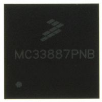
MC33887PNB Freescale Semiconductor, MC33887PNB Datasheet - Page 4

MC33887PNB
Manufacturer Part Number
MC33887PNB
Description
IC H-BRIDGE CURR FDBK 5A 36-PQFN
Manufacturer
Freescale Semiconductor
Type
Half Bridge DC Motor Driverr
Datasheet
1.MCZ33887EKR2.pdf
(37 pages)
Specifications of MC33887PNB
Applications
DC Motor Controller, H Bridge
Number Of Outputs
1
Current - Output
5A
Voltage - Supply
5 V ~ 28 V
Operating Temperature
-40°C ~ 125°C
Mounting Type
Surface Mount
Package / Case
36-PQFN, 36-PowerQFN
Operating Supply Voltage
5 V to 40 V
Mounting Style
SMD/SMT
For Use With
KIT33887PNBEVB - KIT EVAL 33887 5A H-BRIDGE PQFNKIT33887DWBEVB - KIT EVAL 33887 5A H-BRIDGE SOIC
Lead Free Status / RoHS Status
Lead free / RoHS Compliant
Voltage - Load
-
Lead Free Status / Rohs Status
Lead free / RoHS Compliant
Available stocks
Company
Part Number
Manufacturer
Quantity
Price
Company:
Part Number:
MC33887PNB
Manufacturer:
Freescale Semiconductor
Quantity:
805
Part Number:
MC33887PNB
Manufacturer:
FREESCALE
Quantity:
20 000
Company:
Part Number:
MC33887PNBR2
Manufacturer:
TOSHIBA
Quantity:
177
Part Number:
MC33887PNBR2
Manufacturer:
FREESCALE
Quantity:
20 000
4
Table 2. PQFN PIN DEFINITIONS
33887
PIN CONNECTIONS
Transparent Top View of Package
5, 6, 12, 13, 34, 35
A functional description of each pin can be found in the
14, 15, 17, 18
29, 30, 32, 33
1, 7, 10, 16,
19, 28, 31
21– 26
Pad
Pin
11
20
27
36
2
3
4
8
9
Pin Name
Interface
Thermal
AGND
PGND
OUT1
OUT2
CCP
NC
IN2
IN1
D1
EN
FS
FB
D2
V+
Fault Status for H-Bridge
Charge Pump Capacitor
Feedback for H-Bridge
Positive Power Supply
Exposed Pad Thermal
Logic Input Control 2
Logic Input Control 1
H-Bridge Output 1
H-Bridge Output 2
AGND
Analog Ground
Power Ground
Formal Name
No Connect
IN2
NC
NC
NC
EN
D1
FS
V+
V+
Disable 1
Disable 2
Interface
Enable
Figure 4. 33887 Pin Connections
10
1
2
3
4
5
6
7
8
9
Functional Pin DescriptionS
No internal connection to this pin.
Active HIGH input used to simultaneously tri-state disable both H-Bridge
outputs. When D1 is Logic HIGH, both outputs are tri-stated.
Logic input control of OUT2 (i.e., IN2 logic HIGH = OUT2 HIGH).
Logic input Enable control of device (i.e., EN logic HIGH = full operation,
EN logic LOW = Sleep Mode).
Positive supply connections.
Low-current analog signal ground.
Open drain active LOW Fault Status output requiring a pull-up resistor to
5.0 V.
Logic input control of OUT1 (i.e., IN1 logic HIGH = OUT1 HIGH).
Output 1 of H-Bridge.
Current feedback output providing ground referenced 1/375th ratio of
H-Bridge high-side current.
High-current power ground.
Active LOW input used to simultaneously tri-state disable both H-Bridge
outputs. When D2 is Logic LOW, both outputs are tri-stated.
Output 2 of H-Bridge.
External reservoir capacitor connection for internal charge pump
capacitor.
Exposed pad thermal interface for sinking heat from the device.
Note: Must be DC-coupled to analog ground and power ground via very
low impedance path to prevent injection of spurious signals into IC
substrate.
28
27
26
25
24
23
22
21
20
19
NC
D2
PGND
PGND
PGND
PGND
PGND
PGND
FB
NC
section,
Analog Integrated Circuit Device Data
Definition
page
21.
Freescale Semiconductor


