MC3PHACVDWE Freescale Semiconductor, MC3PHACVDWE Datasheet - Page 15
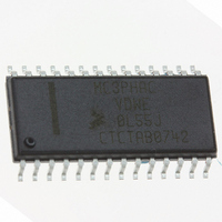
MC3PHACVDWE
Manufacturer Part Number
MC3PHACVDWE
Description
IC MOTOR CONTROLLER 28-SOIC
Manufacturer
Freescale Semiconductor
Datasheet
1.MC3PHACVFAE.pdf
(36 pages)
Specifications of MC3PHACVDWE
Applications
AC Motor Controller, 3 Phase
Number Of Outputs
1
Voltage - Supply
4.5 V ~ 5.5 V
Operating Temperature
-40°C ~ 105°C
Mounting Type
Surface Mount
Package / Case
28-SOIC (7.5mm Width)
Processor Series
MC3PHAC
Core
HC08
Data Bus Width
8 bit
Program Memory Type
Flash
Program Memory Size
8 KB
Data Ram Size
256 KB
Interface Type
SCI
Maximum Clock Frequency
8.2 MHz
Number Of Programmable I/os
14
Number Of Timers
2
Maximum Operating Temperature
+ 85 C
Mounting Style
SMD/SMT
Minimum Operating Temperature
- 40 C
On-chip Adc
10 bit, 4 Channel
Lead Free Status / RoHS Status
Lead free / RoHS Compliant
Current - Output
-
Voltage - Load
-
Lead Free Status / Rohs Status
Details
Available stocks
Company
Part Number
Manufacturer
Quantity
Price
Company:

Part Number:
MC3PHACVDWE
Manufacturer:
NSC
Quantity:
1 430


Digital Power Supply Bypassing
V
Fast signal transitions connected internally on these pins place high, short-duration current demands on
the power supply. To prevent noise problems, take special care to provide power supply bypassing at the
V
frequency-response ceramic capacitor, such as a 0.1 µF, paralleled with a bulk capacitor in the range of
1 µF to 10 µF for bypassing the digital power supply.
Analog Power Supply Bypassing
V
digital converter (ADC). On the schematics in this document, analog ground is labeled with an A and other
grounds are digital grounds. Analog power is labeled as +5 A. It is good practice to isolate the analog and
digital +5 volt power supplies by using a small inductor or a low value resistor less than 5 ohms in series
with the digital power supply, to create the +5 A supply. ADC V
the ADC’s voltage reference.
Decoupling of these pins should be per the digital power supply bypassing, described previously. ADC
V
Grounding Considerations
Printed circuit board layout is an important design consideration. In particular, ground planes and how
grounds are tied together influence noise immunity. To maximize noise immunity, it is important to get a
good ground plane under the MC3PHAC. It is also important to separate analog and digital grounds. That
is why, shown on the schematics, there are two ground designations, analog ground is marked with an A
and other grounds are digital grounds. GND is the digital ground plane and power supply return. GNDA
is the analog circuit ground. They are both the same reference voltage, but are routed separately, and tie
together at only one point.
Power-Up/Power-Down
When power is applied or removed, it is important that the inverter’s top and bottom output transistors in
the same phase are not turned on simultaneously. Since logic states are not always defined during power-
up, it is important to ensure that all power transistors remain off when the controller’s supply voltage is
below its normal operating level. The MC3PHAC’s PWM module outputs make this easy by switching to
a high impedance configuration whenever the 5-volt supply is below its specified minimum.
The user should use pullup or pulldown resistors on the output of the MC3PHAC’s PWM outputs to ensure
during power-up and power-down, that the inverter’s drive inputs are at a known, turned off, state.
Freescale Semiconductor
DD
DD
DDA
REF
and V
and V
(pin 1) and V
and V
SS
SS
SSA
are the digital power supply and ground pins for the MC3PHAC.
pins. Place the bypass capacitors as close as possible to the MC3PHAC. Use a high-
are the power supply pins for the analog portion of the clock generator and analog-to-
DDA
(pin 3) shall be connected together and connected to the same potential as V
MC3PHAC Monolithic Intelligent Motor Controller, Rev. 2
REF
is the power supply pin used for setting
Digital Power Supply Bypassing
DD
15
.
Related parts for MC3PHACVDWE
Image
Part Number
Description
Manufacturer
Datasheet
Request
R

Part Number:
Description:
Mc3phac Motor Control Unit
Manufacturer:
Freescale Semiconductor, Inc
Datasheet:
Part Number:
Description:
Manufacturer:
Freescale Semiconductor, Inc
Datasheet:
Part Number:
Description:
Manufacturer:
Freescale Semiconductor, Inc
Datasheet:
Part Number:
Description:
Manufacturer:
Freescale Semiconductor, Inc
Datasheet:
Part Number:
Description:
Manufacturer:
Freescale Semiconductor, Inc
Datasheet:
Part Number:
Description:
Manufacturer:
Freescale Semiconductor, Inc
Datasheet:
Part Number:
Description:
Manufacturer:
Freescale Semiconductor, Inc
Datasheet:
Part Number:
Description:
Manufacturer:
Freescale Semiconductor, Inc
Datasheet:
Part Number:
Description:
Manufacturer:
Freescale Semiconductor, Inc
Datasheet:
Part Number:
Description:
Manufacturer:
Freescale Semiconductor, Inc
Datasheet:
Part Number:
Description:
Manufacturer:
Freescale Semiconductor, Inc
Datasheet:
Part Number:
Description:
Manufacturer:
Freescale Semiconductor, Inc
Datasheet:
Part Number:
Description:
Manufacturer:
Freescale Semiconductor, Inc
Datasheet:
Part Number:
Description:
Manufacturer:
Freescale Semiconductor, Inc
Datasheet:
Part Number:
Description:
Manufacturer:
Freescale Semiconductor, Inc
Datasheet: