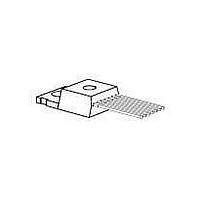
TLE5206-2S Infineon Technologies, TLE5206-2S Datasheet

TLE5206-2S
Specifications of TLE5206-2S
SP000377311
TLE52062S
TLE52062SNK
TLE52062SXK
Available stocks
Related parts for TLE5206-2S
TLE5206-2S Summary of contents
Page 1
H-Bridge for DC-Motor Applications 1 Overview 1.1 Features • Delivers continuous 6 A peak current • Optimized for DC motor management applications • Operates at supply voltages • Very low ...
Page 2
Pin Configuration (top view) TLE 5206 GND V OUT1 IN1 IN2 TLE 5206- OUT1 IN1 IN2 EF GND V S Figure 1 Data Sheet GND 1 N.C. ...
Page 3
Pin Definitions and Functions Pin No. Pin No. Symbol P-TO220 P-DSO 1 7 OUT1 IN1 4 1, 10, GND 11 IN2 OUT2 – ...
Page 4
Functional Block Diagram 2 EF Diagnosis and Protection Circuit 1 3 IN1 5 IN2 Diagnosis and Protection Circuit 2 Figure 2 Block Diagram Data Sheet Error Flag IN OUT ...
Page 5
Circuit Description Input Circuit The control inputs consist of TTL/CMOS-compatible schmitt-triggers with hysteresis. Buffer amplifiers are driven by this stages. Output Stages The output stages consist of a DMOS H-bridge. Integrated circuits protect the outputs against short-circuit to ground ...
Page 6
Monitoring Functions Undervoltage lockout (UVLO): V When reaches the switch on voltage S All output transistors are switched off if the supply voltage V value S OFF. 1.8 Protective Function Various errors like short-circuit to + result in turn-OFF ...
Page 7
Diagnosis Various errors as listed in the table “Diagnosis” are detected. Short circuits and overload result in turning off the output stages after a delay simultaneously [EF = L]. Changing the inputs to a state where the fault is ...
Page 8
Electrical Characteristics 3.1 Absolute Maximum Ratings T – < < 150 C j Parameter Voltages Supply voltage Logic input voltage Diagnostics output voltage Currents of DMOS-Transistors and Freewheeling Diodes Output current (cont.) Output current (peak) Output current ...
Page 9
Operating Range Parameter Supply voltage Supply voltage increasing Supply voltage decreasing Logic input voltage Junction temperature 3.3 Electrical Characteristics 6 V < V < IN1 = IN2 = HIGH (No load); – ...
Page 10
Electrical Characteristics (cont’ < < IN1 = IN2 = HIGH (No load); – < OUT1, 2 Parameter Outputs OUT1, 2 Static Drain-Source-On Resistance Source I = – ...
Page 11
Electrical Characteristics (cont’ < < IN1 = IN2 = HIGH (No load); – < OUT1, 2 Parameter Short Circuit Current Limitation Source current Sink current Output Delay ...
Page 12
Electrical Characteristics (cont’ < < IN1 = IN2 = HIGH (No load); – < OUT1, 2 Parameter Leakage Current Source Sink Logic Control Inputs ...
Page 13
IN1 V IN2 Figure 3 Test Circuit Overcurrent I I OUT SD Data Sheet ; FU S 470 OUT1 IN1 3 TLE 5206-2 IN1 IN2 5 OUT2 IN2 GND 4 ...
Page 14
OUT Source OUT Sink Figure 4 Switching Time Definitions + Figure 5 Application Circuit Data Sheet 50% t dONH 80% 50% 20% t ONH ...
Page 15
Application Modes 1. Simple CW/CCW-Control For low-cost application simple CW/CCW-Control without any speed regulation is recommended. A low-speed two-line interface is sufficient for the brake low, clockwise, counter clockwise and brake high command. 2. Sign/Magnitude Control For this mode two ...
Page 16
IN1, 2 SCH SDH OUT1 OUT1, 2 Short SCH t dSD EF Figure 7 Timing Diagram for Output Shorted to Ground IN1, 2 SCL SDL OUT1 OUT1 Short SCL ...
Page 17
Diagrams Quiescent Current I (active) S versus Junction Temperature - Input Switching Thresholds versus Junction Temperature 3 INH, L INH 2.5 2.0 V INL 1.5 1.0 0.5 ...
Page 18
Overcurrent Shutdown Threshold versus Junction Temperature Low Side Transistor 8 High Side Transistor - Data Sheet I Error-Flag Saturation Output Voltage versus Junction Temperature j EF AED02402 0.6 ...
Page 19
Package Outlines P-TO220-7-11 (Plastic Transistor Single Outline Package) 0...0.3 0...0.15 1) Typical Metal surface min. X=7.25, Y=12.3 All metal surfaces tin plated, except area of cut. Sorts of Packing Package outlines for tubes, trays etc. are contained in our ...
Page 20
P-DSO-20-12 (Plastic Dual Small Outline Package) 1.2 -0.3 1.27 +0.13 0 Index Marking 1 x 45˚ 15.9 1) Does not include plastic or metal protrusion of 0.15 max. per side Sorts of Packing Package outlines for tubes, trays ...
Page 21
P-TO263-7-1 Option E3180 (Plastic Transistor Single Outline Package) 0...0.3 7x0.6 ±0 Typical Metal surface min. X=7.25, Y=6.9 All metal surfaces tin plated, except area of cut. Sorts of Packing Package outlines for tubes, trays etc. are contained in ...
Page 22
P-TO220-7-12 (Plastic Transistor Single Outline Package) 0...0.15 1) Typical Metal surface min. X=7.25, Y=12.3 All metal surfaces tin plated, except area of cut. Sorts of Packing Package outlines for tubes, trays etc. are contained in our Data Book “Package Information”. ...


