MC33887DWB Freescale Semiconductor, MC33887DWB Datasheet - Page 8
MC33887DWB
Manufacturer Part Number
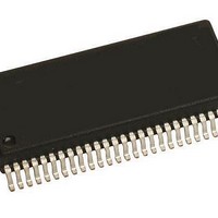
MC33887DWB
Description
IC H-BRIDGE 5.0A W/CS 54-SOIC
Manufacturer
Freescale Semiconductor
Type
Half Bridge DC Motor Driverr
Datasheet
1.MCZ33887EKR2.pdf
(37 pages)
Specifications of MC33887DWB
Applications
DC Motor Controller, H Bridge
Number Of Outputs
1
Current - Output
5A
Voltage - Supply
5 V ~ 28 V
Operating Temperature
-40°C ~ 125°C
Mounting Type
Surface Mount
Package / Case
54-SOIC (7.5mm Width) Exposed Pad, 54-eSOIC, 54-HSOIC
Operating Supply Voltage
5 V to 40 V
Mounting Style
SMD/SMT
For Use With
KIT33887PNBEVB - KIT EVAL 33887 5A H-BRIDGE PQFNKIT33887DWBEVB - KIT EVAL 33887 5A H-BRIDGE SOIC
Lead Free Status / RoHS Status
Contains lead / RoHS non-compliant
Voltage - Load
-
Lead Free Status / Rohs Status
Lead free / RoHS Compliant
Available stocks
Company
Part Number
Manufacturer
Quantity
Price
Company:

Part Number:
MC33887DWBR2
Manufacturer:
TI
Quantity:
27


8
33887
ELECTRICAL CHARACTERISTICS
MAXIMUM RATINGS
MAXIMUM RATINGS (continued)
All voltages are with respect to ground unless otherwise noted.
THERMAL RESISTANCE (AND PACKAGE DISSIPATION) RATINGS
Notes
Junction-to-Board (Bottom Exposed Pad Soldered to Board)
Junction-to-Ambient, Natural Convection, Single-Layer Board (1s)
Junction-to-Ambient, Natural Convection, Four-Layer Board (2s2p)
(14)
Junction-to-Case (Exposed Pad)
10
11
12
13
14
15
9
HSOP (6.0 W)
PQFN (4.0 W)
SOICW-EP (2.0 W)
HSOP (6.0 W)
PQFN (4.0 W)
SOICW-EP (2.0 W)
HSOP (6.0 W)
PQFN (4.0 W)
SOICW-EP (2.0 W)
HSOP (6.0 W)
PQFN (4.0 W)
SOICW-EP (2.0 W)
The limiting factor is junction temperature, taking into account the power dissipation, thermal resistance, and heat sinking.
Exposed heatsink pad plus the power and ground pins comprise the main heat conduction paths. The actual R
values will vary depending on solder thickness and composition and copper trace thickness. Maximum current at maximum die
temperature represents ~ 16 W of conduction loss heating in the diagonal pair of output MOSFETs. Therefore, the R
less than 5.0 °C/W for maximum load at 70°C ambient. Module thermal design must be planned accordingly.
Thermal resistance between the die and the printed circuit board per JEDEC JESD51-8. Board temperature is measured on the top
surface of the board near the package.
Junction temperature is a function of on-chip power dissipation, package thermal resistance, mounting site (board) temperature, ambient
temperature, air flow, power dissipation of other components on the board, and board thermal resistance.
Per SEMI G38-87 and JEDEC JESD51-2 with the single-layer board (JESD51-3) horizontal.
Per JEDEC JESD51-6 with the board horizontal.
Indicates the maximum thermal resistance between the die and the exposed pad surface as measured by the cold plate method (MIL
SPEC-883 Method 1012.1) with the cold plate temperature used for the case temperature.
Rating
(15)
(13)
(9)
,
(10)
Symbol
R
R
R
R
,
θ
(11)
θ
θ
θ
JMA
JB
JA
JC
,
(12)
Analog Integrated Circuit Device Data
Value
~ 0.8
~7.0
~8.0
~9.0
~1.2
~2.0
~ 41
~ 50
~ 62
~ 18
~ 21
~ 23
Freescale Semiconductor
θ
JB
(junction-to-PC board)
θ
JC
-total must be
°C/W
°C/W
°C/W
°C/W
Unit
Related parts for MC33887DWB
Image
Part Number
Description
Manufacturer
Datasheet
Request
R


Part Number:
Description:
Manufacturer:
Freescale Semiconductor, Inc
Datasheet:
Part Number:
Description:
Manufacturer:
Freescale Semiconductor, Inc
Datasheet:
Part Number:
Description:
Manufacturer:
Freescale Semiconductor, Inc
Datasheet:
Part Number:
Description:
Manufacturer:
Freescale Semiconductor, Inc
Datasheet:
Part Number:
Description:
Manufacturer:
Freescale Semiconductor, Inc
Datasheet:
Part Number:
Description:
Manufacturer:
Freescale Semiconductor, Inc
Datasheet:
Part Number:
Description:
Manufacturer:
Freescale Semiconductor, Inc
Datasheet:
Part Number:
Description:
Manufacturer:
Freescale Semiconductor, Inc
Datasheet:
Part Number:
Description:
Manufacturer:
Freescale Semiconductor, Inc
Datasheet:
Part Number:
Description:
Manufacturer:
Freescale Semiconductor, Inc
Datasheet:
Part Number:
Description:
Manufacturer:
Freescale Semiconductor, Inc
Datasheet:
Part Number:
Description:
Manufacturer:
Freescale Semiconductor, Inc
Datasheet:
Part Number:
Description:
Manufacturer:
Freescale Semiconductor, Inc
Datasheet:
Part Number:
Description:
Manufacturer:
Freescale Semiconductor, Inc
Datasheet: