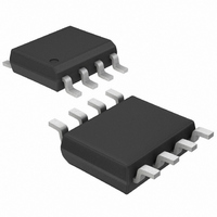
MAX749ESA+ Maxim Integrated Products, MAX749ESA+ Datasheet - Page 2

MAX749ESA+
Manufacturer Part Number
MAX749ESA+
Description
IC SUPPLY LCD BIAS ADJ 8-SOIC
Manufacturer
Maxim Integrated Products
Datasheet
1.MAX749CPA.pdf
(12 pages)
Specifications of MAX749ESA+
Applications
LCD Display
Current - Supply
60µA
Voltage - Supply
2 V ~ 6 V
Operating Temperature
-40°C ~ 85°C
Mounting Type
Surface Mount
Package / Case
8-SOIC (3.9mm Width)
Lead Free Status / RoHS Status
Lead free / RoHS Compliant
ABSOLUTE MAXIMUM RATINGS
V+ ................................................................................-0.3V, +7V
CTRL, ADJ, FB, DLOW, DHI, CS.....................-0.3V, (V+ + 0.3V)
Continuous Power Dissipation (T
ELECTRICAL CHARACTERISTICS
(2V < V+ < 6V, T
TIMING CHARACTERISTICS
Digitally Adjustable LCD Bias Supply
Stresses beyond those listed under “Absolute Maximum Ratings" may cause permanent damage to the device. These are stress ratings only, and functional
operation of the device at these or any other conditions beyond those indicated in the operational sections of the specifications is not implied. Exposure to
absolute maximum rating conditions for extended periods may affect device reliability.
Note 1: The device is in regulation when V
Note 2: These tests performed at V+ = 3.3V. Operation over supply range is guaranteed by supply rejection test of full-count current.
Note 3: V
2
V+ Voltage
FB Source Current
Zero-Count FB Current
Full-Count FB Current
FB Offset Voltage
DAC Step Size (Note 2)
DAC Linearity (Note 2)
Supply Rejection
Switching Frequency
Logic Input Current
Logic High Threshold (Note 3)
Logic Low Threshold (Note 3)
Quiescent Current
Shutdown Current
V+ to CS Voltage
DHI Source Current
DHI Drive Level
DLOW On Resistance
Minimum Reset Pulse Width
Minimum Reset Setup
Minimum Reset Hold
Minimum ADJ High Pulse Width
Minimum ADJ Low Pulse Width
Minimum ADJ Low to CTRL Low
Plastic DIP (derate 9.09mW/°C above +70°C) ............727mW
SO (derate 5.88mW/°C above +70°C) .........................471mW
______________________________________________________________________________________
PARAMETER
T
IH
A
PARAMETER
= T
is guaranteed by design to be 1.8V min for V+ = 2V to 6V for T
MIN
A
= T
to T
MIN
MAX
to T
.
MAX
A
SYMBOL
, unless otherwise noted.)
= +70°C)
I
V
FBS
V
IH
IL
SYMBOL
t
t
t
t
t
t
RH
SH
SD
RS
SL
FB
R
= 0V (see Figures 3 - 6).
On power-up or reset, V
V
V
Monotonicity guaranteed, V
V
V+ = 2V to 6V, full-count current
0V < V
CTRL, ADJ
CTRL, ADJ
Current-limit trip voltage
V+ = 2V, V
No load
V+ = 2V, V
FB
FB
FB
= 0V
= 0V
= 0V
V+ = 2V
V+ = 5V
Not tested
Not tested
V+ = 2V
V+ = 5V
V+ = 2V
V+ = 5V
V+ = 2V
V+ = 5V
IN
CONDITIONS
< V+, CTRL, ADJ
DHI
DLOW
CONDITIONS
= 1V
= 0.5V
FB
Operating Temperature Ranges:
Storage Temperature Range .............................-65°C to +160°C
Lead Temperature (soldering, 10sec) .............................+300°C
MAX749C_A........................................................0°C to +70°C
MAX749E_A .....................................................-40°C to +85°C
= 0V (Note 1)
A
FB
= T
MIN
0
0
= 0V
MIN
T
to T
A
TYP
125
170
= +25°C
25
15
10
60
70
20
MAX
V+ - 50mV
12.80
. V
MIN
0.45
1.43
1.00
110
1.6
24
2
IL
MAX
300
400
150
200
85
85
85
85
is guaranteed by design from
100 to 500
13.33
TYP
1.56
140
V+
50
5
T
A
MIN
= T
0
0
MIN
13.86
±100
MAX
0.55
1.53
2.12
±15
180
1.5
0.4
±1
60
15
10
6
to T
MAX
400
100
100
100
500
200
250
100
MAX
UNITS
%I
%I
%I
I
I
kHz
mV
mV
mA
FBS
FBS
UNITS
µA
nA
µA
µA
Ω
V
V
V
V
FBS
FBS
FBS
ns
ns
ns
ns
ns
ns


