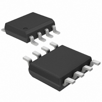
MAX749ESA+ Maxim Integrated Products, MAX749ESA+ Datasheet - Page 6

MAX749ESA+
Manufacturer Part Number
MAX749ESA+
Description
IC SUPPLY LCD BIAS ADJ 8-SOIC
Manufacturer
Maxim Integrated Products
Datasheet
1.MAX749CPA.pdf
(12 pages)
Specifications of MAX749ESA+
Applications
LCD Display
Current - Supply
60µA
Voltage - Supply
2 V ~ 6 V
Operating Temperature
-40°C ~ 85°C
Mounting Type
Surface Mount
Package / Case
8-SOIC (3.9mm Width)
Lead Free Status / RoHS Status
Lead free / RoHS Compliant
Once turned off, a one-shot holds the switch off for a
minimum of 1µs, and the switch either stays off (if the
output is in regulation), or turns on again (if the output
is out of regulation).
With light loads, the transistor switches for one or more
cycles and then turns off, much like a traditional PFM
converter. With heavy loads, the transistor stays on until
the switch current reaches the current limit; it then
shuts off for 1µs, and immediately turns on again until
the next time the switch current reaches its limit. This
cycle repeats until the output is in regulation.
The output voltage is set using a single external resistor
and the internal current-output DAC (Figure 1). The full-
scale output voltage is set by selecting the feedback
resistor, R
to 100% of the full-scale output by an internal 64-step
DAC/counter.
On power-up or after a reset, the counter sets the DAC
output to mid-range. Each rising edge of ADJ incre-
Digitally Adjustable LCD Bias Supply
Figure 2. Switch-Mode Power-Supply Section Block Diagram
6
______________________________________________________________________________________
FB
. The output voltage is controlled from 33%
MAX749
Q
TRIG
MAXIMUM
ONE-SHOT
ONE-SHOT
ON-TIME
MINIMUM
OFF-TIME
TRIG
Q
Output Voltage Control
S
REF
FLIP-FLOP
R
GND
Q
6-BIT
CURRENT-OUTPUT
DAC
COMPARATOR
CURRENT
0.1 F
ments the DAC output. When incremented beyond full
scale, the counter rolls over and sets the DAC to the
minimum value. In this way, a single pulse applied to
ADJ increases the DAC set point by one step, and 63
pulses decrease the set point by one step.
Table 1 is the logic table for the CTRL and ADJ inputs,
which control the internal DAC and counter. Figures 3-7
show various timing specifications and different ways of
incrementing and resetting the DAC, and of placing it in
the low-power standby mode. As long as the timing
specifications for ADJ and CTRL are observed, any
sequence of operations can be implemented.
Table 1. Input Truth Table
140mV
ADJ
High
Low
X
V+
COMPARATOR
VOLTAGE
+2V TO +6V
INPUT
DLOW
CTRL
High
High
Low
Low
DHI
FB
Shut down
Reset counter to mid-range. The
device is not shut down.
On
Increment the counter
R
470
C
BASE
R
COMP
FB
R
SENSE
RESULT
Q1
ZTX750
22 F
30V
L1
47 H
(NEGATIVE)
D1
1N5819
22 F
V
OUT


