ADT7473ARQZ-1R7 ON Semiconductor, ADT7473ARQZ-1R7 Datasheet - Page 57
ADT7473ARQZ-1R7
Manufacturer Part Number
ADT7473ARQZ-1R7
Description
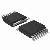
IC THERM MON FAN CTLR 16-QSOP
Manufacturer
ON Semiconductor
Series
dBCool®r
Datasheet
1.ADT7473ARQZ-1RL.pdf
(74 pages)
Specifications of ADT7473ARQZ-1R7
Function
Fan Control, Temp Monitor
Topology
ADC, Comparator, Fan Speed Counter, Multiplexer, Register Bank
Sensor Type
External & Internal
Sensing Temperature
-40°C ~ 125°C, External Sensor
Output Type
SMBus™
Output Alarm
No
Output Fan
Yes
Voltage - Supply
3 V ~ 3.6 V
Operating Temperature
-40°C ~ 125°C
Mounting Type
Surface Mount
Package / Case
16-QSOP
Full Temp Accuracy
+/- 0.5 C
Digital Output - Bus Interface
Serial (3-Wire, 4-Wire)
Maximum Operating Temperature
+ 125 C
Minimum Operating Temperature
- 40 C
Lead Free Status / RoHS Status
Lead free / RoHS Compliant
Available stocks
Company
Part Number
Manufacturer
Quantity
Price
Company:

Part Number:
ADT7473ARQZ-1R7
Manufacturer:
ON Semiconductor
Quantity:
500
Part Number:
ADT7473ARQZ-1R7
Manufacturer:
ADI/亚德诺
Quantity:
20 000


Table 18. Temperature Reading Registers (Power−On Default = 0x01)
1. These temperature readings can be in twos complement or Offset 64 format; this interpretation is determined by Bit 0 of Configuration
2. If the extended resolution bits of these readings are also being read, the extended resolution registers (Register 0x76 and Register 0x77)
3. In twos complement mode, a temperature reading of −128°C (0x80) indicates a diode fault (open or short) on that channel.
4. In Offset 64 mode, a temperature reading of −64°C (0x00) indicates a diode fault (open or short) on that channel.
Table 19. Fan Tachometer Reading Registers (Power−On Default = 0x00)
1. These registers count the number of 11.11 ms periods (based on an internal 90 kHz clock) that occur between a number of consecutive fan
Table 20. Current PWM Duty Cycle Registers (ADT7473 Power−On Default = 0x00,
ADT7473−1 Power−On Default = 0xFF)
1. These registers reflect the PWM duty cycle driving each fan at any given time. When in automatic fan speed control mode, the
Table 21. Operating Point Registers (Power−On = 0xA4)
1. These registers set the target operating point for each temperature channel when the dynamic T
2. The fans being controlled are adjusted to maintain temperature about an operating point.
3. These registers become read−only when the Configuration Register 1 lock bit is set to 1. Any subsequent attempts to write to these
Register Address
Register Address
Register Address
Register Address
Register 5 (0x7C).
must be read first. Once the extended resolution registers have been read, all associated MSB reading registers are frozen until read. Both
the extended resolution registers and the MSB registers are frozen.
TACH pulses (default = 2). The number of TACH pulses used to count can be changed using the TACH pulses per revolution register (Register
0x7B). This allows the fan speed to be accurately measured. Because a valid fan tachometer reading requires that two bytes are read, the
low byte must be read first. Both the low and high bytes are then frozen until read. At power−on, these registers contain 0x0000 until the first
valid fan TACH measurement is read into these registers. This prevents false interrupts from occurring while the fans are spinning up. A count
of 0xFFFF indicates a fan is one of the following:
• Stalled or blocked (object jamming the fan).
• Failed (internal circuitry destroyed).
• Not populated. (The ADT7473/ADT7473−1 expects to see a fan connected to each TACH. If a fan is not connected to that TACH, its TACH
minimum high and low bytes should be set to 0xFFFF.)
• Alternate function, for example, TACH4 reconfigured as THERM pin.
ADT7473/ADT7473−1 reports the PWM duty cycles back through these registers. The PWM duty cycle values vary according to
temperature in automatic fan speed control mode. During fan startup, these registers report back 0x00. In software mode, the PWM duty
cycle outputs can be set to any duty cycle value by writing to these registers.
registers fail.
0x2A
0x2B
0x2C
0x2D
0x2E
0x25
0x26
0x27
0x28
0x29
0x2F
0x30
0x31
0x32
0x33
0x34
0x35
R/W (Note 3)
Read−only
Read−only
Read−only
Read−only
Read−only
Read−only
Read−only
Read−only
Read−only
Read−only
Read−only
R/W
R/W
R/W
R/W
R/W
R/W
R/W
R/W
R/W
Remote 1 temperature reading (8 MSB of reading). (Note 3 and 4)
Local temperature reading (8 MSB of reading).
Remote 2 temperature reading (8 MSB of reading). (Note 3 and 4)
TACH1 low byte.
TACH1 high byte.
TACH2 low byte.
TACH2 high byte.
TACH3 low byte.
TACH3 high byte.
TACH4 low byte.
TACH4 high byte.
PWM1 current duty cycle (0% to 100% duty cycle = 0x00 to 0xFF).
PWM2 current duty cycle (0% to 100% duty cycle = 0x00 to 0xFF).
PWM3 current duty cycle (0% to 100% duty cycle = 0x00 to 0xFF).
Remote 1 operating point register (default = 100°C).
Local temperature operating point register (default = 100°C).
Remote 2 operating point register (default = 100°C).
(Note 1)
http://onsemi.com
57
(Note 1, 2 and 3)
(Note 1 and 2)
Description
Description
Description
Description
(Note 1)
MIN
control feature is enabled.
Related parts for ADT7473ARQZ-1R7
Image
Part Number
Description
Manufacturer
Datasheet
Request
R

Part Number:
Description:
ON Semiconductor [VOLTAGE REGULATOR]
Manufacturer:
ON Semiconductor
Datasheet:
Part Number:
Description:
357-036-542-201 CARDEDGE 36POS DL .156 BLK LOPRO
Manufacturer:
ON Semiconductor
Datasheet:
Part Number:
Description:
357-036-542-201 CARDEDGE 36POS DL .156 BLK LOPRO
Manufacturer:
ON Semiconductor
Datasheet:
Part Number:
Description:
357-036-542-201 CARDEDGE 36POS DL .156 BLK LOPRO
Manufacturer:
ON Semiconductor
Datasheet:
Part Number:
Description:
357-036-542-201 CARDEDGE 36POS DL .156 BLK LOPRO
Manufacturer:
ON Semiconductor
Datasheet:
Part Number:
Description:
357-036-542-201 CARDEDGE 36POS DL .156 BLK LOPRO
Manufacturer:
ON Semiconductor
Datasheet:
Part Number:
Description:
357-036-542-201 CARDEDGE 36POS DL .156 BLK LOPRO
Manufacturer:
ON Semiconductor
Datasheet:
Part Number:
Description:
357-036-542-201 CARDEDGE 36POS DL .156 BLK LOPRO
Manufacturer:
ON Semiconductor
Datasheet:
Part Number:
Description:
357-036-542-201 CARDEDGE 36POS DL .156 BLK LOPRO
Manufacturer:
ON Semiconductor
Datasheet:
Part Number:
Description:
357-036-542-201 CARDEDGE 36POS DL .156 BLK LOPRO
Manufacturer:
ON Semiconductor
Datasheet:
Part Number:
Description:
357-036-542-201 CARDEDGE 36POS DL .156 BLK LOPRO
Manufacturer:
ON Semiconductor
Datasheet:
Part Number:
Description:
Manufacturer:
ON Semiconductor
Datasheet:
Part Number:
Description:
Manufacturer:
ON Semiconductor
Datasheet:
Part Number:
Description:
Manufacturer:
ON Semiconductor
Datasheet: