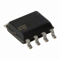
UC3842BD1013TR STMicroelectronics, UC3842BD1013TR Datasheet - Page 2

UC3842BD1013TR
Manufacturer Part Number
UC3842BD1013TR
Description
IC PWM CTRLR CURR MODE 8-SOIC
Manufacturer
STMicroelectronics
Datasheet
1.UC3845BD1013TR.pdf
(15 pages)
Specifications of UC3842BD1013TR
Pwm Type
Current Mode
Number Of Outputs
1
Frequency - Max
500kHz
Duty Cycle
100%
Voltage - Supply
11.5 V ~ 25 V
Buck
No
Boost
Yes
Flyback
Yes
Inverting
No
Doubler
No
Divider
No
Cuk
No
Isolated
Yes
Operating Temperature
0°C ~ 70°C
Package / Case
8-SOIC (3.9mm Width)
Frequency-max
500kHz
Duty Cycle (max)
100 %
Output Voltage
5.10 V
Output Current
1000 mA (Max)
Mounting Style
SMD/SMT
Switching Frequency
500 KHz
Operating Supply Voltage
30 V
Maximum Operating Temperature
150 C
Fall Time
50 ns
Minimum Operating Temperature
- 40 C
Rise Time
50 ns
Synchronous Pin
No
Topology
Boost or Flyback or Forward
Lead Free Status / RoHS Status
Lead free / RoHS Compliant
Other names
497-6139-2
Available stocks
Company
Part Number
Manufacturer
Quantity
Price
Company:
Part Number:
UC3842BD1013TR
Manufacturer:
ST
Quantity:
30 000
Part Number:
UC3842BD1013TR
Manufacturer:
ST
Quantity:
20 000
* All voltages are with respect to pin 5, all currents are positive into the specified terminal.
UC2842B/3B/4B/5B - UC3842B/3B/4B/5B
ABSOLUTE MAXIMUM RATINGS
PIN CONNECTION (top view)
PIN FUNCTIONS
ORDERING NUMBERS
2/15
Symbol
No
1
2
3
4
5
6
7
8
T
P
P
E
T
T
V
V
I
O
stg
tot
tot
O
J
L
i
i
GROUND
Function
OUTPUT
COMP
I
R
SENSE
V
V
V
T
Supply Voltage (low impedance source)
Supply Voltage (Ii < 30mA)
Output Current
Output Energy (capacitive load)
Analog Inputs (pins 2, 3)
Error Amplifier Output Sink Current
Power Dissipation at T
Power Dissipation at Tamb
Storage Temperature Range
Junction Operating Temperature
Lead Temperature (soldering 10s)
CC
/C
FB
ref
UC2842BD1; UC3842BD1
UC2843BD1; UC3843BD1
UC2844BD1; UC3844BD1
UC2845BD1; UC3845BD1
T
This pin is the Error Amplifier output and is made available for loop compensation.
This is the inverting input of the Error Amplifier. It is normally connected to the switching
power supply output through a resistor divider.
A voltage proportional to inductor current is connected to this input. The PWM uses this
information to terminate the output switch conduction.
The oscillator frequency and maximum Output duty cycle are programmed by connecting
resistor R
This pin is the combined control circuitry and power ground.
This output directly drives the gate of a power MOSFET. Peak currents up to 1A are sourced
and sunk by this pin.
This pin is the positive supply of the control IC.
This is the reference output. It provides charging current for capacitor C
SO8
T
to Vref and cpacitor C
amb
COMP
I
R
SENSE
T
V
/C
Parameter
FB
T
25 C (Minidip)
25 C (SO8)
1
2
3
4
Minidip/SO8
D95IN332
T
to ground. Operation to 500kHz is possible.
8
7
6
5
Description
V
Vi
OUTPUT
GROUND
REF
UC2842BN; UC3842BN
UC2843BN; UC3843BN
UC2844BN; UC3844BN
UC2845BN; UC3845BN
Minidip
Self Limiting
– 0.3 to 5.5
– 65 to 150
– 40 to 150
Value
1.25
800
300
30
10
5
1
T
through resistor R
Unit
mW
mA
°C
W
V
A
V
C
C
J
T
.


