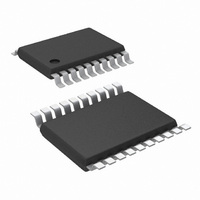
LM5035MHX/NOPB National Semiconductor, LM5035MHX/NOPB Datasheet - Page 16

LM5035MHX/NOPB
Manufacturer Part Number
LM5035MHX/NOPB
Description
IC PWM BCK BST FLYBK INV 20TSSOP
Manufacturer
National Semiconductor
Series
PowerWise®r
Datasheet
1.LM5035SQNOPB.pdf
(28 pages)
Specifications of LM5035MHX/NOPB
Pwm Type
Voltage Mode
Number Of Outputs
1
Frequency - Max
1MHz
Duty Cycle
92%
Voltage - Supply
13 V ~ 105 V
Buck
Yes
Boost
Yes
Flyback
Yes
Inverting
Yes
Doubler
No
Divider
No
Cuk
No
Isolated
Yes
Operating Temperature
-40°C ~ 125°C
Package / Case
20-TSSOP Exposed Pad, 20-eTSSOP, 20-HTSSOP
Frequency-max
2MHz
For Use With
LM5035EVAL - BOARD EVALUATION LM5035
Lead Free Status / RoHS Status
Lead free / RoHS Compliant
Other names
LM5035MHX
Available stocks
Company
Part Number
Manufacturer
Quantity
Price
Company:
Part Number:
LM5035MHX/NOPB
Manufacturer:
NS/TI
Quantity:
3 775
www.national.com
Synchronous Rectifier Control
Outputs (SR1 & SR2)
Synchronous rectification (SR) of the transformer secondary
provides higher efficiency, especially for low output voltage
converters. The reduction of rectifier forward voltage drop
(0.5V - 1.5V) to 10mV - 200mV V
significantly reduces rectification losses. In a typical applica-
tion, the transformer secondary winding is center tapped, with
the output power inductor in series with the center tap. The
SR MOSFETs provide the ground path for the energized sec-
ondary winding and the inductor current. Figure 5 shows that
the SR2 MOSFET is conducting while HO enables power
transfer from the primary. The SR1 MOSFET must be dis-
abled during this period since the secondary winding con-
nected to the SR1 MOSFET drain is twice the voltage of the
center tap. At the conclusion of the HO pulse, the inductor
current continues to flow through the SR1 MOSFET body
diode. Since the body diode causes more loss than the SR
MOSFET, efficiency can be improved by minimizing the T2
period while maintaining sufficient timing margin over all con-
ditions (component tolerances, etc.) to prevent shoot-through
current. When LO enables power transfer from the primary,
the SR1 MOSFET is enabled and the SR2 MOSFET is off.
During the time that neither HO nor LO is active, the inductor
current is shared between both the SR1 and SR2 MOSFETs
which effectively shorts the transformer secondary and can-
cels the inductance in the windings. The SR2 MOSFET is
disabled before LO delivers power to the secondary to pre-
vent power being shunted to ground. The SR2 MOSFET body
diode continues to carry about half the inductor current until
the primary power raises the SR2 MOSFET drain voltage and
reverse biases the body diode. Ideally, dead-time T1 would
be set to the minimum time that allows the SR MOSFET to
turn off before the SR MOSFET body diode starts conducting.
The SR1 and SR2 outputs are powered directly by the VCC
regulator. Each output is capable of sourcing and sinking 0.5A
DS
voltage for a MOSFET
FIGURE 5. HO, LO, SR1 and SR2 Timing Diagram
16
peak. Typically, the SR1 and SR2 signals control SR MOS-
FET gate drivers through a pulse transformer. The actual gate
sourcing and sinking currents are provided by the secondary-
side bias supply and gate drivers.
The timing of SR1 and SR2 with respect to HO and LO is
shown in Figure 5. SR1 is configured out of phase with HO
and SR2 is configured out of phase with LO. The deadtime
between transitions is programmable by a resistor connected
from the DLY pin to the AGND pin. Typically, R
the range of 10kΩ to 100kΩ. The deadtime periods can be
calculated using the following formulae:
To set the minimum (propagation delays only) deadtime, the
DLY pin should be left open or connected to the REF pin. Any
resistor value above 300kΩ connected between the DLY pin
and AGND will also provide the minimum period (approxi-
mately 5 ns).
Thermal Protection
Internal Thermal Shutdown circuitry is provided to protect the
integrated circuit in the event the maximum rated junction
temperature is exceeded. When activated, typically at 165°C,
the controller is forced into a low power standby state with the
output drivers (HO, LO, SR1 and SR2), the bias regulators
(VCC and REF) disabled. This helps to prevent catastrophic
failures from accidental device overheating. During thermal
shutdown, the soft-start capacitor is fully discharged and the
controller follows a normal start-up sequence after the junc-
tion temperature falls to the operating level (145°C).
T1 = [R
T2 = [R
DLY
DLY
x 2.8ps] + 20ns
x 1.35ps] + 6ns
20177521
DLY
is set in


