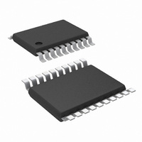
LM5035MHX/NOPB National Semiconductor, LM5035MHX/NOPB Datasheet - Page 21

LM5035MHX/NOPB
Manufacturer Part Number
LM5035MHX/NOPB
Description
IC PWM BCK BST FLYBK INV 20TSSOP
Manufacturer
National Semiconductor
Series
PowerWise®r
Datasheet
1.LM5035SQNOPB.pdf
(28 pages)
Specifications of LM5035MHX/NOPB
Pwm Type
Voltage Mode
Number Of Outputs
1
Frequency - Max
1MHz
Duty Cycle
92%
Voltage - Supply
13 V ~ 105 V
Buck
Yes
Boost
Yes
Flyback
Yes
Inverting
Yes
Doubler
No
Divider
No
Cuk
No
Isolated
Yes
Operating Temperature
-40°C ~ 125°C
Package / Case
20-TSSOP Exposed Pad, 20-eTSSOP, 20-HTSSOP
Frequency-max
2MHz
For Use With
LM5035EVAL - BOARD EVALUATION LM5035
Lead Free Status / RoHS Status
Lead free / RoHS Compliant
Other names
LM5035MHX
Available stocks
Company
Part Number
Manufacturer
Quantity
Price
Company:
Part Number:
LM5035MHX/NOPB
Manufacturer:
NS/TI
Quantity:
3 775
The typical operating ranges of undervoltage and overvoltage
thresholds are calculated from the above equations. For ex-
ample, for resistor values R1 = 86.6kΩ, R2 = 2.10kΩ and R3
= 1.40kΩ the computed thresholds are:
To maintain the threshold’s accuracy, a resistor tolerance of
1% or better is recommended.
The design process starts with the choice of the voltage dif-
ference between the UVLO enabling and disabling thresh-
olds. This will also approximately set the difference between
OVP enabling and disabling regulation:
Next, the combined resistance of R
choosing the threshold for the UVLO disabling threshold:
Then R
old:
Finally, R
Outputs disabled due to VIN falling below UVLO threshold
Outputs enabled due to VIN rising above UVLO threshold
Outputs disabled due to VIN rising above OVP threshold
Outputs enabled due to VIN falling below OVP threshold
3
is determined by selecting the OVP disabling thresh-
3
is subtracted from R
COMBINED
2
and R
FIGURE 13. Remote Standby and Disable Control
to give R
3
TABLE 1. UVO/OVP Divider Formulas
is calculated by
2
:
21
UVLO
OVP
UVLO turn-off = 32.2V
UVLO turn-on = 34.2V
OVP turn-on = 78.4V
OVP turn-off = 80.5V
Remote configuration of the controller’s operational modes
can be accomplished with open drain device(s) connected to
the UVLO pin as shown in Figure 13.
FAULT PROTECTION
The Over Voltage Protection (OVP) comparator of the
LM5035 can be configured for line or load fault protection or
thermal protection using an external temperature sensor or
thermistor. Figure 11 shows a line over voltage shutdown ap-
plication using a voltage divider between the input power
supply, V
Figure 14 demonstrates the use of the OVP pin for latched
output over-voltage fault protection, using a zener and opto-
coupler. When V
opto-coupler diode and zener, the opto-coupler momentarily
turns on Q1 and the LM5035 enters standby mode, disabling
the drivers and enabling the hysteresis current source on the
OVP pin. Once the current source is enabled, the OVP volt-
age will remain at 2.3V (23µA x 100kΩ) without additional
drive from the external circuit. If the opto-coupler transistor
emitter were directly connected to the OVP pin, then leakage
current in the zener diode amplified by the opto-coupler’s gain
could falsely trip the protection latch. R1 and Q1 are added
reduce the sensitivity to low level currents in the opto-coupler.
Using the values of Figure 14, the opto-coupler collector cur-
rent must equal V
on
on
= OVP
= UVLO
PWR
off
- [23µA x (R1 + R2)]
, and AGND to monitor the line voltage.
off
+ (23µA x R
OUT
BE(Q1)
R
exceeds the conduction threshold of the
2
= R
/ R1 = 350µA before OVP latches.
COMBINED
1
)
- R
20177536
3
www.national.com


