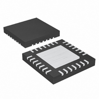
MAX1536ETI+ Maxim Integrated Products, MAX1536ETI+ Datasheet - Page 13

MAX1536ETI+
Manufacturer Part Number
MAX1536ETI+
Description
IC PWM STEP-DN DC-DC CONV 28TQFN
Manufacturer
Maxim Integrated Products
Type
Step-Down (Buck), PWM - Current Moder
Datasheet
1.MAX1536ETIT.pdf
(19 pages)
Specifications of MAX1536ETI+
Internal Switch(s)
Yes
Synchronous Rectifier
Yes
Number Of Outputs
1
Voltage - Output
0.7 ~ 5.5 V
Current - Output
3.6A
Frequency - Switching
1.4MHz
Voltage - Input
3 ~ 5.5 V
Operating Temperature
-40°C ~ 85°C
Mounting Type
*
Package / Case
28-TQFN Exposed Pad
Voltage - Supply
3 V ~ 5.5 V
Frequency-max
1.4MHz
Duty Cycle
100%
Pwm Type
Current Mode
Buck
Yes
Boost
No
Flyback
No
Inverting
No
Doubler
No
Divider
No
Cuk
No
Isolated
No
Lead Free Status / RoHS Status
Lead free / RoHS Compliant
The MAX1536 features a thermal fault-protection circuit.
When the junction temperature rises above +165°C, a
thermal sensor shuts down the MAX1536 regardless of
V
temperature cools to +150°C.
Junction-to-ambient thermal resistance, θ
dependent on the amount of copper area connected to
the exposed backside pad. Airflow over the board sig-
nificantly reduces θ
ly distribute the copper area connected at the IC among
the high-current pins. Refer to the Maxim website
(www.maxim-ic.com) for QFN thermal considerations.
Power dissipation in the MAX1536 is dominated by
conduction losses in the two internal power switches.
Power dissipation due to supply current in the control
section and average current used to charge and dis-
charge the gate capacitance of the internal switches
(i.e., switching losses—P
where:
C = 5nF.
f
The combined conduction losses (P
power switches are approximated by:
where:
I
R
Figure 4. Maximum Recommended Operating Frequency vs.
Input Voltage
SW
OUT
Down Regulator with Dynamic Output Voltage Control
PMOS
SHDN
= switching frequency.
= load current.
. The MAX1536 is reactivated after the junction
= PMOS switch on-resistance.
1800
1600
1400
1200
1000
800
600
400
200
3.6A, 1.4MHz, Low-Voltage, Internal-Switch Step-
0
3.0
V
OUT
V
P
P
OUT
______________________________________________________________________________________
CL
SL
= 1.5V
JA
3.5
= 2.5V
= I
. For heat-sinking purposes, even-
= C x V
V
OUT 2
OUT
SL
V
4.0
OUT
= 3.3V
V
) is approximately:
IN
= 1.8V
(V)
IN 2
Thermal Resistance
x R
4.5
Thermal Shutdown
Power Dissipation
x f
PMOS
V
OUT
SW
NO LOAD
5.0
= 1.0V
CL
5.5
) in the two
JA
, is highly
The junction-to-ambient thermal resistance required to
dissipate this amount of power is calculated by:
where:
θ
T
T
For typical applications, use the recommended compo-
nent values in Table 1. For other applications, take the
following steps:
1) Select the desired PWM-mode switching frequency.
2) Select the constant off-time as a function of input
3) Select R
4) Select the inductor as a function of output voltage,
The MAX1536 output voltage (V
and REFIN (Figure 5). The MAX1536 regulates V
be equal to V
divider between V
+0.7V to V
calculate R
Figure 5. Setting V
JA
J(MAX)
A(MAX)
Setting V
See Figure 4 for maximum operating frequency.
voltage, output voltage, and switching frequency.
off-time, and peak-to-peak inductor current.
0.22µF
V
= junction-to-ambient thermal resistance.
OUT
C
V
REF
REF
= V
= maximum junction temperature = +150°C.
= +2.0V
= maximum ambient temperature.
FB
(
OUT
1 +
IN
A
TOFF
R
. Select an R
R
based on the desired V
B
θ
A
REFIN
)
JA
with a Resistive Voltage-Divider at FB
OUT
REF
REFIN
as a function of off-time.
≤
OUT
. Connect FB to a resistive voltage-
T
MAX1536
with a Resistive Voltage-Divider at FB
J MAX
Setting the Output Voltage
(
P
and AGND to adjust V
SL
)
PGND
AGND
B
+
-
Design Procedure
T
LX
FB
P
from 10kΩ to 100kΩ, then
A MAX
CL
(
V
FB
OUT
= V
)
REFIN
OUT
) is set using FB
:
V
OUT
OUT
= +2.5V
R
2.49kΩ
R
10kΩ
A
B
FB
from
13
to


