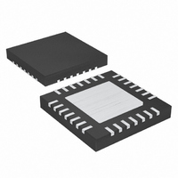
MAX1536ETI+ Maxim Integrated Products, MAX1536ETI+ Datasheet - Page 16

MAX1536ETI+
Manufacturer Part Number
MAX1536ETI+
Description
IC PWM STEP-DN DC-DC CONV 28TQFN
Manufacturer
Maxim Integrated Products
Type
Step-Down (Buck), PWM - Current Moder
Datasheet
1.MAX1536ETIT.pdf
(19 pages)
Specifications of MAX1536ETI+
Internal Switch(s)
Yes
Synchronous Rectifier
Yes
Number Of Outputs
1
Voltage - Output
0.7 ~ 5.5 V
Current - Output
3.6A
Frequency - Switching
1.4MHz
Voltage - Input
3 ~ 5.5 V
Operating Temperature
-40°C ~ 85°C
Mounting Type
*
Package / Case
28-TQFN Exposed Pad
Voltage - Supply
3 V ~ 5.5 V
Frequency-max
1.4MHz
Duty Cycle
100%
Pwm Type
Current Mode
Buck
Yes
Boost
No
Flyback
No
Inverting
No
Doubler
No
Divider
No
Cuk
No
Isolated
No
Lead Free Status / RoHS Status
Lead free / RoHS Compliant
The MAX1536 is optimized to work in applications that
require two dynamic output voltages; however, discrete
logic or a DAC connected to REFIN allows three or
more dynamic output voltages.
Figure 6 shows an application circuit providing four
voltage levels using discrete logic. Switching resistors
in and out of the resistor network changes the voltage
at REFIN. An edge-detection circuit is added to trigger
a 1µs pulse on GATE to start the fault-blanking and
forced-PWM operation. GATE requires a minimum
pulse width of 500ns. The edge-detection circuit is not
required if the MAX1536 is always in PWM mode (SKIP
= V
Active bus termination power supplies generate a volt-
age rail that tracks a set reference. Active bus termina-
tion power supplies are unique because they source
and sink current. DDR memory architecture requires
active bus termination. In DDR memory architecture,
the termination voltage is set at exactly half the memory
supply voltage. Configure the MAX1536 to generate the
termination voltage using a resistor-divider at REFIN.
Force the MAX1536 to operate in PWM mode (SKIP =
V
MAX1536 configured as a DDR termination regulator.
Connect GATE and FBLANK to AGND when unused.
3.6A, 1.4MHz, Low-Voltage, Internal-Switch Step-
Down Regulator with Dynamic Output Voltage Control
Figure 6. Multioutput Voltage Settings
16
CC
B
A
CC
) to source and sink current. Figure 7 shows the
______________________________________________________________________________________
) and fault blanking is not necessary.
1.5kΩ
1.5kΩ
Applications Information
R4
Multioutput Voltage Settings
1000pF
1000pF
R3
Active Bus Termination
C1
R1
R2
REF
REFIN
AGND
OD
OD
GATE
MAX1536
Good layout is necessary to achieve the intended out-
put power level, high efficiency, and low noise. Good
layout includes the use of a ground plane, careful com-
ponent placement, and correct routing of traces using
appropriate trace widths. Refer to the MAX1536 EV Kit
for layout reference.
Figure 7. Active Bus Termination
Figure 8. Source/Sink Waveforms
1000pF
1000pF
V
DDQ
0
0
V
IN
= 3.3V, V
V
10kΩ
10kΩ
CC
OUT
Circuit Layout and Grounding
SKIP
REFIN
AGND
GATE
FBLANK
= 1.25V, I
MAX1536
10µs/div
OUT
= -1A TO +1A TO -1A
PGND
V
V
OD
OD
FB
LX
DDQ
TT
IN
= TERMINATION SUPPLY VOLTAGE
= DDR MEMORY SUPPLY VOLTAGE
L
V
50mV/div
V
5V/div
I
2A/div
LX
OUT
LX
C
C
OUT
V
IN
TT
=
V
V
DDQ
IN
2


