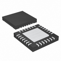
MAX1536ETI+ Maxim Integrated Products, MAX1536ETI+ Datasheet - Page 14

MAX1536ETI+
Manufacturer Part Number
MAX1536ETI+
Description
IC PWM STEP-DN DC-DC CONV 28TQFN
Manufacturer
Maxim Integrated Products
Type
Step-Down (Buck), PWM - Current Moder
Datasheet
1.MAX1536ETIT.pdf
(19 pages)
Specifications of MAX1536ETI+
Internal Switch(s)
Yes
Synchronous Rectifier
Yes
Number Of Outputs
1
Voltage - Output
0.7 ~ 5.5 V
Current - Output
3.6A
Frequency - Switching
1.4MHz
Voltage - Input
3 ~ 5.5 V
Operating Temperature
-40°C ~ 85°C
Mounting Type
*
Package / Case
28-TQFN Exposed Pad
Voltage - Supply
3 V ~ 5.5 V
Frequency-max
1.4MHz
Duty Cycle
100%
Pwm Type
Current Mode
Buck
Yes
Boost
No
Flyback
No
Inverting
No
Doubler
No
Divider
No
Cuk
No
Isolated
No
Lead Free Status / RoHS Status
Lead free / RoHS Compliant
3.6A, 1.4MHz, Low-Voltage, Internal-Switch Step-
Down Regulator with Dynamic Output Voltage Control
where V
The MAX1536 regulates V
Changing V
that changes between two set points (see the
Multioutput Voltage Settings section for information on
three or more output-voltage set points). Figure 1 shows
a dynamically adjustable resistive voltage-divider net-
work at REFIN. Keep V
Keep V
age lockout condition. Toggling GATE switches in and
out the resistor connected between OD and AGND
changing V
internal N-channel MOSFET, forcing OD to a low-imped-
ance state. A low logic on GATE turns off the internal N-
channel MOSFET, making OD high impedance. The
output voltage is determined by the following equations:
The MAX1536 automatically enters forced-PWM opera-
tion on the rising and falling edges of GATE, and
remains in forced-PWM mode for a minimum time
selected by FBLANK (Table 3). Forced-PWM operation
is required to ensure fast, accurate negative voltage
transitions when REFIN is lowered. Since forced-PWM
operation disables the zero-crossing comparator, the
inductor current can reverse under light loads, quickly
discharging the output capacitors. The MAX1536 also
forces PGOOD to a high-impedance state for the peri-
od selected by FBLANK (Table 3).
For a step-voltage change at REFIN, the rate of change
of the output voltage is limited by the inductor current
ramp, the total output capacitance, the current limit,
and the load during the transition. The voltage across
the inductor and the inductance limits the inductor cur-
rent ramp. The total output capacitance determines
how much current is needed to change the output volt-
age. Additional load current slows down the output volt-
age change during a positive REFIN voltage change,
14
14
______________________________________________________________________________________
______________________________________________________________________________________
REFIN
Setting Dynamic Output Voltages with REFIN
FB
= V
REFIN
REFIN
V
V
V
below V
OUT
FB LOW
FB HIGH
REFIN
R
(
(
A
. A logic high on GATE turns on the
=
=
allows for a dynamic output voltage
.
V
R
)
)
FB
=
B
CC
=
V
V
V
REF
1
REFIN
REF
V
- 1.35V to avoid an undervolt-
OUT
+
FB
FB
R
R
A
B
R
R
-
1
1
1
to be equal to V
between 0.7V and 2V.
R
R
+
+
2
2
R
R
+
2
2
R
+
3
R
3
REFIN
.
and speeds up the output voltage change during a
negative REFIN voltage change.
Adding a capacitor across REFIN and AGND filters
noise and controls the rate of change of the REFIN volt-
age during dynamic transitions. With the additional
capacitance, the REFIN voltage slews between the two
set points with a time constant given by the equivalent
parallel resistance seen by the slew capacitor C
As shown in Figure 1, the time constant for a positive
REFIN voltage transition is:
and the time constant for a negative REFIN voltage
transition is:
During a negative REFIN voltage transition, the MAX1536
sinks current to discharge the output capacitor and bring
the output voltage down to the new set point. The
MAX1536 does not have a negative current limit, so
τ
rent within the maximum current capability of the IC:
The MAX1536 features a programmable PWM mode
switching frequency, which is set by the input and out-
put voltage and the value of R
PMOS power switch off-time in PWM mode. Use the fol-
lowing equation to select the off-time according to the
desired no-load switching frequency in PWM mode:
where:
t
V
V
f
Select R
OFF
PWM
NEG
IN
OUT
= the input voltage.
= the programmed off-time.
= no-load switching frequency, PWM mode.
must be set long enough to keep the sinking cur-
= the output voltage.
Programming the No-Load Switching
TOFF
τ
NEG
τ
according to the formula:
POS
≥
τ
NEG
t
C
=
OFF
OUT
R x R
=
R
=
I
1
SINK
1
x V
f
R
V
R x R
+
PWM
∆
Frequency and Off-Time
1
(
1
IN
R
+
2
OUT
2
-
R
V
x V
+
+
2
2
OUT
R
R
and I
IN
3
3
C
TOFF
)
REFIN
C
SINK
REFIN
. R
TOFF
≤
I
LIMIT
sets the
REFIN
.


