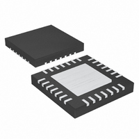
MAX1536ETI+ Maxim Integrated Products, MAX1536ETI+ Datasheet - Page 8

MAX1536ETI+
Manufacturer Part Number
MAX1536ETI+
Description
IC PWM STEP-DN DC-DC CONV 28TQFN
Manufacturer
Maxim Integrated Products
Type
Step-Down (Buck), PWM - Current Moder
Datasheet
1.MAX1536ETIT.pdf
(19 pages)
Specifications of MAX1536ETI+
Internal Switch(s)
Yes
Synchronous Rectifier
Yes
Number Of Outputs
1
Voltage - Output
0.7 ~ 5.5 V
Current - Output
3.6A
Frequency - Switching
1.4MHz
Voltage - Input
3 ~ 5.5 V
Operating Temperature
-40°C ~ 85°C
Mounting Type
*
Package / Case
28-TQFN Exposed Pad
Voltage - Supply
3 V ~ 5.5 V
Frequency-max
1.4MHz
Duty Cycle
100%
Pwm Type
Current Mode
Buck
Yes
Boost
No
Flyback
No
Inverting
No
Doubler
No
Divider
No
Cuk
No
Isolated
No
Lead Free Status / RoHS Status
Lead free / RoHS Compliant
3.6A, 1.4MHz, Low-Voltage, Internal-Switch Step-
Down Regulator with Dynamic Output Voltage Control
8
22, 23,
24, 26
19, 20
27, 28
1, 21,
8, 25
2, 3,
PIN
10
11
12
13
14
15
16
17
18
4
5
6
7
9
_______________________________________________________________________________________
FBLANK
PGOOD
NAME
COMP
AGND
SHDN
REFIN
PGND
GATE
TOFF
SKIP
N.C.
V
REF
OD
OD
LX
FB
IN
CC
Inductor Connection. Connection for the drains of the PMOS power switch and NMOS synchronous-rectifier
switch. Connect all LX pins together.
Power Input. Power input for the internal PMOS switch. Connect all IN pins together.
Shutdown Control Input. Drive SHDN low to disable the reference, control circuitry, and internal MOSFETs.
Drive SHDN high or connect to V
Pulse-Skipping Control Input. Connect SKIP to V
for high-efficiency Idle Mode.
Feedback Input. The voltage at REFIN sets the feedback regulation voltage (V
Integrator Compensation. Connect a 470pF capacitor from COMP to V
See the Integrator Amplifier section.
No Connection. Not internally connected. Connecting pin 25 to LX eases PC board layout.
Off-Time Select Input. Sets the PMOS power switch off-time during constant off-time operation. Connect a
resistor from TOFF to AGND to adjust the PMOS switch off-time. See the Programming the No-Load Switching
Frequency and Off-Time section.
Buffered OD and OD Control Input. A logic low on GATE forces OD low and OD high impedance. A logic high
on GATE forces OD high impedance and OD low.
Open-Drain Output. A logic low on GATE forces OD high impedance. A logic high on GATE forces OD low.
Inverted Open-Drain Output. A logic low on GATE forces OD low. A logic high on GATE forces OD high
impedance.
External Reference Input. The voltage at REFIN sets the feedback regulation voltage (V
+2.0V Reference Voltage Output. Bypass REF to AGND with a minimum capacitance of 0.22µF. REF supplies
up to 50µA for external loads. The internal reference turns off in shutdown.
Analog Ground. Connect backside pad to AGND.
Analog Power Input. Power input to the internal analog circuitry. Bypass V
lowpass filter (Figure 1).
Fault-Blanking Control Input. FBLANK is a four-level logic input that enables or disables fault blanking, and sets
the minimum forced-PWM operation time (t
time period after a transition is detected on GATE. Additionally, the controller enters forced-PWM mode for the
duration of t
fault blanking:
V
Open = 100µs (typ), fault blanking enabled
REF = 50µs (typ), fault blanking enabled
AGND = 100µs (typ), fault blanking disabled
Open-Drain Power-Good Output. PGOOD is low during soft-start, in shutdown, and when the output voltage is
more than 10% (typ) above or below the normal regulation point. After the soft-start, PGOOD becomes high
impedance if the output is in regulation. PGOOD is blanked—forced into a high-impedance state—when
FBLANK is enabled and a transition is detected on GATE.
Power Ground. Internally connected to the source of the internal NMOS synchronous-rectifier switch.
Connect all PGND pins together.
CC
= 150µs (typ), fault blanking enabled
FBLANK
anytime GATE changes states. Connect FBLANK to the following pins to select t
CC
for normal operation.
FBLANK
CC
). Enabling fault blanking forces PGOOD high for the selected
FUNCTION
for low-noise, forced-PWM mode. Connect SKIP to AGND
CC
CC
for integrator compensation.
with a 10Ω and 2.2µF (min)
FB
= V
REFIN
Pin Description
FB
).
= V
REFIN
).
FBLANK
and


