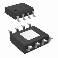
LP2998MR/NOPB National Semiconductor, LP2998MR/NOPB Datasheet

LP2998MR/NOPB
Specifications of LP2998MR/NOPB
Available stocks
Related parts for LP2998MR/NOPB
LP2998MR/NOPB Summary of contents
Page 1
... Suspend To RAM (STR) functionality. When SD is pulled low, the V state providing a high impedance output, while V active. A power savings advantage can be obtained in this mode through lower quiescent current. Typical Application Circuit © 2011 National Semiconductor Corporation LP2998 Features ■ Source and sink current ■ ...
Page 2
Connection Diagrams Pin Descriptions SO-8 Pin or PSOP-8 Pin Ordering Information Order Number Package Type LP2998MA LP2998MAX LP2998MAE LP2998MR PSOP-8 LP2998MRX PSOP-8 LP2998MRE PSOP-8 www.national.com Top View PSOP-8 Layout Top View SO-8 ...
Page 3
... Absolute Maximum Ratings If Military/Aerospace specified devices are required, please contact the National Semiconductor Sales Office/ Distributors for availability and specifications. AVIN to GND PVIN to GND VDDQ (Note 2) Storage Temp. Range Junction Temperature Lead Temperature (Soldering, 10 sec) SO-8 Thermal Resistance (θ PSOP-8 Thermal Resistance (θ ...
Page 4
Symbol Parameter V Output Voltage (DDR Output Voltage (DDR II Output Voltage (DDR III Output Voltage Offset ( Output Voltage Offset (V TT VOS Vtt V Output Voltage Offset ...
Page 5
Symbol Parameter I V Input current SENSE SENSE T Thermal Shutdown (Note Thermal Shutdown Hysteresis SD_HYS Note 1: Absolute maximum ratings indicate limits beyond which damage to the device may occur. Operating range indicates conditions for which ...
Page 6
Typical Performance Characteristics and DDQ www.national.com Unless otherwise specified VIN = AVIN = PVIN = 2.5V 30026920 IL 30026922 30026926 30026921 V ...
Page 7
over Temperature IN 30026928 Maximum Sinking Current 1.8V) DDQ 30026936 Maximum Sourcing Current 2.5V 2.5V) DDQ IN 30026932 Maximum Sourcing Current ...
Page 8
Maximum Sinking Current 2.5V) DDQ www.national.com Maximum Sourcing Current DDQ 30026934 1.8V 3.3V) IN 30026937 ...
Page 9
Block Diagram Description The LP2998 is a linear bus termination regulator designed to meet the JEDEC requirements of SSTL-2 and SSTL-18. The output capable of sinking and sourcing current while TT regulating the output voltage equal to VDDQ ...
Page 10
V . Care should be taken when a long implemented in close proximity to the memory. Noise pick the V trace can cause problems with precise SENSE regulation small ...
Page 11
Figure 2 varies with airflow for JA the two boards mentioned. FIGURE 2. θ vs Airflow (SO-8) JA Additional improvements can be made by the judicious use of vias to connect the part and dissipate ...
Page 12
Typical Application Circuits Several different application circuits have been shown in ure 3 through Figure 12 to illustrate some of the options that are possible in configuring the LP2998. Graphs of the indi- vidual circuit performance can be found in ...
Page 13
FIGURE 5. SSTL-2 Implementation With Higher Voltage Rails DDR-II APPLICATIONS With the separate VDDQ pin and an internal resistor divider it is possible to use the LP2998 in applications utilizing DDR- II memory. Figure 6 and Figure 7 show several ...
Page 14
LEVEL SHIFTING If standards other than SSTL-2 are required, such as SSTL-3, it may be necessary to use a different scaling factor than 0.5 times V for regulating the output voltage. Several options DDQ are available to scale the output ...
Page 15
QDR APPLICATIONS Quad data rate (QDR) applications utilize multiple channels for improved memory performance. However, this increase in bus lines increases the current levels required for termination. The recommended approach in terminating multiple channels is to use a dedicated LP2998 ...
Page 16
PCB Layout Considerations 1. The input capacitor for the power rail should be placed as close as possible to the PVIN pin should be connected to the V SENSE at the point where regulation is required. For motherboard ...
Page 17
Physical Dimensions inches (millimeters) unless otherwise noted 8-Lead Small Outline Package (M8) NS Package Number M08A 8-Lead PSOP Package (PSOP-8) NS Package Number MRA08A 17 www.national.com ...
Page 18
... For more National Semiconductor product information and proven design tools, visit the following Web sites at: www.national.com Products Amplifiers www.national.com/amplifiers Audio www.national.com/audio Clock and Timing www.national.com/timing Data Converters www.national.com/adc Interface www.national.com/interface LVDS www.national.com/lvds Power Management www.national.com/power Switching Regulators www.national.com/switchers LDOs www.national.com/ldo LED Lighting www ...


