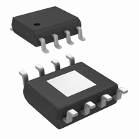
LP2998MR/NOPB National Semiconductor, LP2998MR/NOPB Datasheet - Page 5

LP2998MR/NOPB
Manufacturer Part Number
LP2998MR/NOPB
Description
IC REG TERM VOLT DDRI/II 8-PSOP
Manufacturer
National Semiconductor
Datasheet
1.LP2998MRNOPB.pdf
(18 pages)
Specifications of LP2998MR/NOPB
Applications
Converter, DDR, DDR2, DDR3
Voltage - Input
2.2 ~ 5.5 V
Number Of Outputs
1
Operating Temperature
-40°C ~ 125°C
Mounting Type
Surface Mount
Package / Case
8-PSOP
Primary Input Voltage
2.5V
No. Of Outputs
1
No. Of Pins
8
Output Current
1.5A
Operating Temperature Range
-40°C To +125°C
Msl
MSL 3 - 168 Hours
Filter Terminals
SMD
Rohs Compliant
Yes
For Use With
LP2998EVAL - BOARD EVALUATION FOR LP2998
Lead Free Status / RoHS Status
Lead free / RoHS Compliant
Voltage - Output
-
Other names
LP2998MR
Available stocks
Company
Part Number
Manufacturer
Quantity
Price
Company:
Part Number:
LP2998MR/NOPB
Manufacturer:
TI/NSC
Quantity:
16 500
Part Number:
LP2998MR/NOPB
Manufacturer:
TI/德州仪器
Quantity:
20 000
Symbol
T
I
SD_HYS
SENSE
Note 1: Absolute maximum ratings indicate limits beyond which damage to the device may occur. Operating range indicates conditions for which the device is
intended to be functional, but does not guarantee specific performance limits. For guaranteed specifications and test conditions see Electrical Characteristics.
The guaranteed specifications apply only for the test conditions listed. Some performance characteristics may degrade when the device is not operated under
the listed test conditions.
Note 2: VDDQ voltage must be less than 2 x (AVIN - 1) or 6V, whichever is smaller.
Note 3: The human body model is a 100 pF capacitor discharged through a 1.5 kΩ resistor into each pin.
Note 4: At elevated temperatures, devices must be derated based on thermal resistance. The device in the SO-8 package must be derated at θ
junction to ambient with no heat sink.
Note 5: Limits are 100% production tested at 25°C. Limits over the operating temperature range are guaranteed through correlation using Statistical Quality
Control (SQC) methods. The limits are used to calculate National's Average Outgoing Quality Level (AOQL).
Note 6: Quiescent current is defined as the current flow into AVIN.
Note 7: The maximum allowable power dissipation is a function of the maximum junction temperature, T
and the ambient temperature, T
shutdown.
Note 8: V
T
SD
V
Thermal Shutdown
Thermal Shutdown Hysteresis
TT
SENSE
load regulation is tested by using a 10 ms current pulse and measuring V
Input current
A
. Exceeding the maximum allowable power dissipation will cause excessive die temperature and the regulator will go into thermal
(Note
Parameter
7)
5
TT
.
Conditions
J(MAX)
, the junction to ambient thermal resistance, θ
Min
Typ
165
13
10
JA
www.national.com
Max
= 151.2° C/W
Units
JA
nA
°C
°C
,


