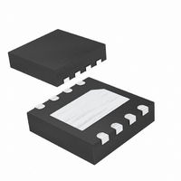
MAX8752ETA+T Maxim Integrated Products, MAX8752ETA+T Datasheet - Page 10

MAX8752ETA+T
Manufacturer Part Number
MAX8752ETA+T
Description
IC DC-DC CONV TFT LCD 8-TDFN
Manufacturer
Maxim Integrated Products
Datasheet
1.MAX8752ETAT.pdf
(12 pages)
Specifications of MAX8752ETA+T
Applications
Converter, TFT, LCD
Voltage - Input
1.8 ~ 5.5 V
Number Of Outputs
1
Voltage - Output
1.8 ~ 13 V
Operating Temperature
0°C ~ 85°C
Mounting Type
Surface Mount
Package / Case
8-TDFN Exposed Pad
Lead Free Status / RoHS Status
Lead free / RoHS Compliant
Choosing an LIR of 0.5 and estimating efficiency of
80% at this operating point:
Using the circuit’s minimum input voltage (2.2V) and
estimating efficiency of 75% at that operating point:
The ripple current and the peak current are:
The total output voltage ripple has two components: the
capacitive ripple caused by the charging and discharg-
ing of the output capacitance, and the ohmic ripple due
to the capacitor’s equivalent series resistance (ESR):
where I
Inductor Selection section). For ceramic capacitors, the
output voltage ripple is typically dominated by
V
teristics of the output capacitor must also be considered.
TFT LCD Step-Up DC-DC Converter
10
RIPPLE(C)
L
I
=
RIPPLE
______________________________________________________________________________________
V
⎛
⎜
⎝
RIPPLE C
2 5
V
10
I
PEAK
IN DC MAX
RIPPLE
.
V
. The voltage rating and temperature charac-
(
I
V
RIPPLE ESR
V
PEAK
⎞
⎟
⎠
=
( )
2
,
is the peak inductor current (see the
⎛
⎜
⎝
2 6
0 23
.
=
(
2 2
≈
.
=
.
)
μ
10
V
H
Output Capacitor Selection
1 4
V
C
RIPPLE C
I
A
=
)
MAIN
V
.
OUT
×
×
≈
×
A
−
0 23
2 2
10
.
(
.
10
I
1 2
+
PEAK
2 5
⎛
⎜
⎝
( )
.
V
V
.
V
V
A
MHz
0 55
V
MAIN
V
×
×
.
MAIN OSC
−
×
+
2
1 2
R
0 75
2 2
10
A
V
.
⎞
⎟
⎠
.
ESR COUT
.
RIPPLE ESR
−
MHz
f
⎛
⎜
⎝
V
V
≈
0 80
0 50
(
)
V
.
.
≈
IN
1 7
.
(
⎞
⎟
⎠
1 4
⎞
⎟ ≈
⎠
≈
A
,
.
)
and
0 55
A
)
.
2 6
.
A
μ
H
The input capacitor (C
drawn from the input supply and reduces noise injec-
tion into the IC. A 10µF ceramic capacitor is used in the
Typical Applications Circuit (Figure 1) because of the
high source impedance seen in typical lab setups.
Actual applications usually have much lower source
impedance since the step-up regulator often runs
directly from the output of another regulated supply.
Typically, C
the Typical Applications Circuit. Ensure a low noise
supply at IN by using adequate C
greater voltage variation can be tolerated on C
decoupled from C
and C3 in Figure 1).
The MAX8752’s high switching frequency demands a
high-speed rectifier. Schottky diodes are recommend-
ed for most applications because of their fast recovery
time and low forward voltage. The diode should be
rated to handle the output voltage and the peak switch
current. Make sure that the diode’s peak current rating
is at least I
section and that its breakdown voltage exceeds the
output voltage.
The MAX8752 operates with an adjustable output from
V
output (V
FB (see Figure 1). Select R2 in the 10kΩ to 50kΩ range.
Calculate R1 with the following equation:
where V
is 1.24V (typ). Place R1 and R2 close to the IC.
IN
to 13V. Connect a resistive voltage-divider from the
FB
MAIN
, the step-up regulator’s feedback set point,
IN
PEAK
) to GND with the center tap connected to
can be reduced below the values used in
R
1
=
calculated in the Inductor Selection
IN
R
using an RC lowpass filter (see R3
2
IN
×
) reduces the current peaks
⎛
⎜
⎝
V
Input Capacitor Selection
MAIN
Output Voltage Selection
V
Rectifier Diode Selection
FB
−
1
IN
⎞
⎟
⎠
. Alternatively,
IN
if IN is


