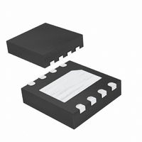
MAX8752ETA+T Maxim Integrated Products, MAX8752ETA+T Datasheet - Page 6

MAX8752ETA+T
Manufacturer Part Number
MAX8752ETA+T
Description
IC DC-DC CONV TFT LCD 8-TDFN
Manufacturer
Maxim Integrated Products
Datasheet
1.MAX8752ETAT.pdf
(12 pages)
Specifications of MAX8752ETA+T
Applications
Converter, TFT, LCD
Voltage - Input
1.8 ~ 5.5 V
Number Of Outputs
1
Voltage - Output
1.8 ~ 13 V
Operating Temperature
0°C ~ 85°C
Mounting Type
Surface Mount
Package / Case
8-TDFN Exposed Pad
Lead Free Status / RoHS Status
Lead free / RoHS Compliant
TFT LCD Step-Up DC-DC Converter
Figure 1. Typical Applications Circuit
6
_______________________________________________________________________________________
PIN
BP
1
2
3
4
5
6
7
8
+1.8V TO +5.5V
-9V/20mA
NAME
COMP
SHDN
V
GND
LDO
SUP
V
GOFF
1.2nF
FB
LX
IN
IN
—
C4
0.1 μ F
10 μ F
6.3V
C1
C8
40.2k Ω
Compensation Pin for Error Amplifier. Connect a series resistance and capacitor from COMP to GND.
See the Loop Compensation section for component selection guidelines.
Feedback Pin. The FB regulation voltage is 1.24V nominal. Connect an external resistive voltage-
divider between the step-up regulator’s output (V
FB. Place the divider close to the IC and minimize the trace area to reduce noise coupling. Set V
according to the Output Voltage Selection section.
Shutdown Control Input. Drive SHDN low to turn off the MAX8752.
Ground
Switching Node. LX is the drain of the internal MOSFET. Connect the inductor/rectifier diode junction
to LX and minimize the trace area for lower EMI.
Supply Pin. Connect IN to the input supply through a series 100Ω resistor and bypass it to GND with
0.1µF or greater ceramic capacitor.
Internal 5V Linear-Regulator Output. This regulator powers all internal circuitry. Bypass LDO to GND
with a 0.22µF or greater ceramic capacitor.
Linear-Regulator Supply Input. SUP is the supply input of the internal 5V linear regulator. Connect
SUP to the step-up regulator output and bypass SUP to GND with a 0.1µF capacitor.
Backside Paddle. Connect the backside paddle to analog ground.
R3
0.22μF
0.1 μ F
100 Ω
20pF
C14
C3
C6
R4
D2
IN
COMP
LDO
0.1 μ F
2.6μH
C9
L1
SHDN
MAX8752
LX
GND
SUP
FB
0.1 μ F
0.1 μ F
C11
C10
D1
FUNCTION
C7
0.1 μ F
MAIN
D3
R1
90.9k Ω
1%
R2
13k Ω
1%
) and GND, with the center tap connected to
D4
C12
0.1 μ F
C13
0.1 μ F
C2
10 μ F
16V
Pin Description
+10V/240mA
28V/10mA
V
V
MAIN
GON
MAIN


