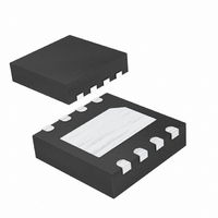
MAX8752ETA+T Maxim Integrated Products, MAX8752ETA+T Datasheet - Page 9

MAX8752ETA+T
Manufacturer Part Number
MAX8752ETA+T
Description
IC DC-DC CONV TFT LCD 8-TDFN
Manufacturer
Maxim Integrated Products
Datasheet
1.MAX8752ETAT.pdf
(12 pages)
Specifications of MAX8752ETA+T
Applications
Converter, TFT, LCD
Voltage - Input
1.8 ~ 5.5 V
Number Of Outputs
1
Voltage - Output
1.8 ~ 13 V
Operating Temperature
0°C ~ 85°C
Mounting Type
Surface Mount
Package / Case
8-TDFN Exposed Pad
Lead Free Status / RoHS Status
Lead free / RoHS Compliant
The maximum output current, input voltage, output volt-
age, and switching frequency determine the inductor
value. Very high inductance values minimize the cur-
rent ripple and therefore reduce the peak current,
which decreases core losses in the inductor and I
losses in the entire power path. However, large induc-
tor values also require more energy storage and more
turns of wire, which increase physical size and can
increase I
ues decrease the physical size but increase the current
ripple and peak current. Finding the best inductor
involves choosing the best compromise between circuit
efficiency, inductor size, and cost.
The equations used here include a constant, LIR, which
is the ratio of the inductor peak-to-peak ripple current
to the average DC inductor current at the full-load cur-
rent. The best trade-off between inductor size and cir-
cuit efficiency for step-up regulators generally has an
LIR between 0.3 and 0.5. However, depending on the
AC characteristics of the inductor core material and
ratio of inductor resistance to other power path resis-
tances, the best LIR can shift up or down. If the induc-
tor resistance is relatively high, more ripple can be
accepted to reduce the number of turns required and
increase the wire diameter. If the inductor resistance is
relatively low, increasing inductance to lower the peak
current can decrease losses throughout the power
path. If extremely thin high-resistance inductors are
used, as is common for LCD panel applications, the
best LIR can increase to between 0.5 and 1.0.
Once a physical inductor is chosen, higher and lower
values of the inductor should be evaluated for efficien-
cy improvements in typical operating regions.
In Figure 1, the LCD’s gate-on and gate-off voltages
are generated from two unregulated charge pumps dri-
ven by the step-up regulator’s LX node. The additional
load on LX must therefore be considered in the induc-
tance calculation. The effective maximum output cur-
rent I
current on the step-up regulator’s output plus the con-
tributions from the positive and negative charge
pumps:
where I
n
n
I
NEG
NEG
POS
I
MAIN(EFF)
MAIN(EFF)
is the negative charge-pump output current, and
is the number of positive charge-pump stages,
is the number of negative charge-pump stages,
MAIN(MAX)
2
R losses in the inductor. Low inductance val-
= I
I
MAIN(MAX)
POS
becomes the sum of the maximum load
_______________________________________________________________________________________
is the maximum main output current,
+ η
NEG
TFT LCD Step-Up DC-DC Converter
x I
NEG
+ (η
POS
+ 1) x
2
R
I
assuming the pump source for I
Calculate the approximate inductor value using the typ-
ical input voltage (V
(I
an appropriate curve in the Typical Operating
Characteristics, and an estimate of LIR based on the
above discussion:
Choose an available inductor value from an appropriate
inductor family. Calculate the maximum DC input cur-
rent at the minimum input voltage V
servation of energy and the expected efficiency at that
operating point (η
in the Typical Operating Characteristics:
Calculate the ripple current at that operating point and
the peak current required for the inductor:
The inductor’s saturation current rating and the
MAX8752’s LX current limit (I
and the inductor’s DC current rating should exceed
I
with less than 0.1Ω series resistance.
Considering the Typical Applications Circuit (Figure 1),
the maximum load current (I
10V output and a typical input voltage of 2.5V:
POS
IN(DC,MAX)
I
MAIN(MAX)
MAIN(EFF)
L
is the positive charge-pump output current,
I
RIPPLE
=
I
IN DC MAX
⎛
⎜
⎝
(
V
I
PEAK
), the expected efficiency (η
. For good efficiency, choose an inductor
= 180mA + 1 x 20mA + 3 x 10mA = 230mA
MAIN
V
IN
,
=
⎞
⎟
⎠
V
2
MIN
=
)
IN MIN
⎛
⎜
⎝
(
I
I
=
IN DC MAX
MAIN MAX
IN
) taken from an appropriate curve
L
(
), the maximum output current
I
V
MAIN MAX
)
MAIN
×
V
(
,
×
IN MIN
V
MAIN(MAX)
(
(
(
MAIN
V
LIM
MAIN
)
)
−
POS
×
)
+
) should exceed I
)
V
× η
IN
×
f
×
I
OSC
RIPPLE
is V
−
IN(MIN)
f
OSC
V
MIN
2
) is 180mA with a
MAIN
V
MAIN.
TYP
⎞
⎟
⎠
IN MIN
(
⎛
⎜
⎝
) taken from
η
LIR
using con-
TYP
)
)
⎞
⎟
⎠
PEAK
9


