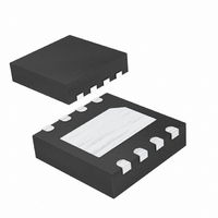
MAX8752ETA+T Maxim Integrated Products, MAX8752ETA+T Datasheet - Page 11

MAX8752ETA+T
Manufacturer Part Number
MAX8752ETA+T
Description
IC DC-DC CONV TFT LCD 8-TDFN
Manufacturer
Maxim Integrated Products
Datasheet
1.MAX8752ETAT.pdf
(12 pages)
Specifications of MAX8752ETA+T
Applications
Converter, TFT, LCD
Voltage - Input
1.8 ~ 5.5 V
Number Of Outputs
1
Voltage - Output
1.8 ~ 13 V
Operating Temperature
0°C ~ 85°C
Mounting Type
Surface Mount
Package / Case
8-TDFN Exposed Pad
Lead Free Status / RoHS Status
Lead free / RoHS Compliant
The voltage-feedback loop needs proper compensa-
tion to prevent excessive output ripple and poor effi-
ciency caused by instability. This is done by
connecting a resistor (R
in series from COMP to GND, and another capacitor
(C
the high-frequency integrator gain for fast transient
response, while C
zero to maintain loop stability. The second capacitor,
C
output-capacitance ESR. For optimal performance,
choose the components using the following equations:
For the ceramic output capacitor, where ESR is small,
C
compensation is by inspecting the transient response
of the MAX8752. Adjust R
sary to obtain optimal transient performance.
Careful PC board layout is important for proper opera-
tion. Use the following guidelines for good PC board
layout:
1) Minimize the area of high-current loops by placing
COMP2
COMP2
COMP2
the inductor, rectifier diode, and output capacitors
near the input capacitors and near the LX and GND
pins. The high-current input loop goes from the
positive terminal of the input capacitor to the induc-
tor, to the IC’s LX pin, out the IC’s GND pin, and to
the input capacitor’s negative terminal. The high-
current output loop is from the positive terminal of
the input capacitor to the inductor, to the rectifier
diode (D1), to the positive terminal of the output
capacitors, reconnecting between the output-
C
COMP
R
C
COMP
COMP
, is chosen to cancel the zero introduced by
) from COMP to GND. R
is optional. The best gauge of correct loop
2
≈
PC Board Layout and Grounding
≈
≈
0 02
264
______________________________________________________________________________________
COMP
10
.
×
×
×
COMP
I
is chosen to set the integrator
MAIN MAX
L
V
R
V
COMP
IN
OUT
ESR
×
V
IN
×
Loop Compensation
I
(
) and capacitor (C
MAIN EFF
×
×
×
TFT LCD Step-Up DC-DC Converter
V
and C
COMP
OUT
V
C
)
L
OUT
(
OUT
×
×
×
COMP
)
R
I
is chosen to set
MAIN EFF
COMP
C
OUT
(
as neces-
)
COMP
)
2) Create a power ground island (PGND) consisting of
3) Place the feedback voltage-divider resistors as
4) Place the SUP and LDO bypass capacitors and the
5) Minimize the length and maximize the width of the
6) Minimize the size of the LX node while keeping it
Refer to the MAX8752 evaluation kit for an example of
proper board layout.
TRANSISTOR COUNT: 3091
PROCESS: BiCMOS
capacitor and input-capacitor ground terminals.
Connect these loop components with short, wide
connections. Avoid using vias in the high-current
paths, especially the ground paths. If vias are
unavoidable, use many vias in parallel to reduce
resistance and inductance.
the input and output capacitor grounds and GND.
Connect all of these together with short, wide traces
or a small ground plane. Maximizing the width of
the power ground traces improves efficiency and
reduces output voltage ripple and noise spikes.
Create an analog ground plane (AGND) consisting
of the feedback divider’s ground, the COMP capac-
itor’s ground, and the IC’s exposed backside pad
near pin 1. Connect the AGND and PGND islands
by connecting the GND pin directly to the exposed
backside pad. Make no other connections between
these separate ground planes.
close to FB as possible. The divider’s center trace
should be kept short. Placing the resistors far away
causes the FB trace to become an antenna that can
pick up switching noise. Avoid running the feed-
back trace near LX.
IN bypass capacitors (C3 in Figure 1) if within 5mm
of their respective pins. Connect their ground termi-
nals to GND through the IC’s exposed back paddle
near GND (pin4).
traces between the output capacitors and the load
for best transient responses.
wide and short. Keep the LX node away from the
feedback node and other sensitive nodes. Use DC
traces as shield if necessary.
Chip Information
11


