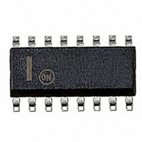
ADP3162JR-REEL ON Semiconductor, ADP3162JR-REEL Datasheet - Page 5

ADP3162JR-REEL
Manufacturer Part Number
ADP3162JR-REEL
Description
IC REG BUCK 5BIT 2PHASE 16-SOIC
Manufacturer
ON Semiconductor
Datasheet
1.ADP3162JRZ-REEL7.pdf
(12 pages)
Specifications of ADP3162JR-REEL
Rohs Status
RoHS non-compliant
Applications
Controller, Intel Tualatin
Voltage - Input
5V, 12V
Number Of Outputs
2
Voltage - Output
1.05 ~ 1.83 V
Operating Temperature
0°C ~ 70°C
Mounting Type
Surface Mount
Package / Case
16-SOIC (3.9mm Width)
Available stocks
Company
Part Number
Manufacturer
Quantity
Price
Company:
Part Number:
ADP3162JR-REEL
Manufacturer:
RTC
Quantity:
50 000
Part Number:
ADP3162JR-REEL
Manufacturer:
ADI/亚德诺
Quantity:
20 000
VID25
0
1
0
1
0
1
0
1
0
1
0
1
0
1
0
1
0
1
0
1
0
1
0
1
0
1
0
1
0
1
0
1
4.7nF
5-BIT CODE
1k
VID3
0
0
0
0
0
0
0
0
0
0
1
1
1
1
1
1
1
1
1
1
1
1
1
1
1
1
0
0
0
0
0
0
Table I. Output Voltage vs. VID Code
VID2
1
1
0
0
0
0
0
0
0
0
1
1
1
1
1
1
1
1
0
0
0
0
0
0
0
0
1
1
1
1
1
1
1
2
3
4
5
6
7
8
VID3
VID2
VID1
VID0
VID25
COMP
FB
CT
AD820
ADP3162
PWRGD
VID1
0
0
1
1
1
1
0
0
0
0
1
1
1
1
0
0
0
0
1
1
1
1
0
0
0
0
1
1
1
1
0
0
PWM1
PWM2
GND
VCC
REF
CS–
CS+
1.2V
16
15
14
13
12
11
10
9
VID0
0
0
1
1
0
0
1
1
0
0
1
1
0
0
1
1
0
0
1
1
0
0
1
1
0
0
1
1
0
0
1
1
+
1 F
V
FB
100nF
V
1.050 V
1.075 V
1.100 V
1.125 V
1.150 V
1.175 V
1.200 V
1.225 V
1.250 V
1.275 V
1.300 V
1.325 V
1.350 V
1.375 V
1.400 V
1.425 V
1.450 V
1.475 V
1.500 V
1.525 V
1.550 V
1.575 V
1.600 V
1.625 V
1.650 V
1.675 V
1.700 V
1.725 V
1.750 V
1.775 V
1.800 V
1.825 V
OUT(NOM)
12V
THEORY OF OPERATION
The ADP3162 combines a current-mode, fixed frequency PWM
controller with antiphase logic outputs in a controller for a two-
phase synchronous buck power converter. Two-phase operation
is important for switching the high currents required by high
performance microprocessors. Handling the high current in a
single-phase converter would place difficult requirements on the
power components such as inductor wire size, MOSFET ON-
resistance and thermal dissipation. The ADP3162’s high side
current sensing topology ensures that the load currents are bal-
anced in each phase, such that neither phase has to carry more
than half of the power. An additional benefit of high side current
sensing over output current sensing is that the average current
through the sense resistor is reduced by the duty cycle of the
converter allowing the use of a lower power, lower cost resistor.
The outputs of the ADP3162 are logic drivers only and are
not intended to directly drive external power MOSFETs.
Instead, the ADP3162 should be paired with drivers such as
the ADP3412, ADP3413, or ADP3414.
The frequency of the ADP3162 is set by an external capacitor
connected to the CT pin. Each output phase of the ADP3162
operates at half of the frequency set by the CT pin. The error
amplifier and current sense comparator control the duty cycle of
the PWM outputs to maintain regulation. The maximum duty
cycle per phase is inherently limited to 50% because the PWM
outputs toggle in two-phase operation. While one phase is on,
the other phase is off. In no case can both outputs be high at the
same time.
Output Voltage Sensing
The output voltage is sensed at the FB pin allowing for remote
sensing. To maintain the accuracy of the remote sensing, the
GND pin should also be connected close to the load. A voltage
error amplifier (g
voltage and a programmable reference voltage. The reference
voltage is programmed between 1.05 V and 1.825 V by an internal
5-bit DAC, which reads the code at the voltage identification
(VID) pins. (Refer to Table I for the output voltage versus VID pin
code information.)
Active Voltage Positioning
The ADP3162 uses Analog Devices Optimal Positioning Tech-
nology (ADOPT), a unique supplemental regulation technique
that uses active voltage positioning and provides optimal com-
pensation for load transients. When implemented, ADOPT adjusts
the output voltage as a function of the load current, so that it is
always optimally positioned for a load transient. Standard (passive)
voltage positioning has poor dynamic performance, rendering
it ineffective under the stringent repetitive transient conditions
required by high performance processors. ADOPT, however,
provides optimal bandwidth for transient response that yields
optimal load transient response with the minimum number of
output capacitors.
Reference Output
A 3.0 V reference is available on the ADP3162. This reference
is normally used to set the voltage positioning accurately using a
resistor divider to the COMP pin. In addition, the reference can
be used for other functions such as generating a regulated voltage
with an external amplifier. The reference is bypassed with a 1 nF
capacitor to ground. It is not intended to supply current to large
capacitive loads, and it should not be used to provide more than
1 mA of output current.
m
) amplifies the difference between the output
ADP3162


