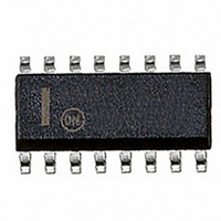
ADP3162JR-REEL ON Semiconductor, ADP3162JR-REEL Datasheet - Page 6

ADP3162JR-REEL
Manufacturer Part Number
ADP3162JR-REEL
Description
IC REG BUCK 5BIT 2PHASE 16-SOIC
Manufacturer
ON Semiconductor
Datasheet
1.ADP3162JRZ-REEL7.pdf
(12 pages)
Specifications of ADP3162JR-REEL
Rohs Status
RoHS non-compliant
Applications
Controller, Intel Tualatin
Voltage - Input
5V, 12V
Number Of Outputs
2
Voltage - Output
1.05 ~ 1.83 V
Operating Temperature
0°C ~ 70°C
Mounting Type
Surface Mount
Package / Case
16-SOIC (3.9mm Width)
Available stocks
Company
Part Number
Manufacturer
Quantity
Price
Company:
Part Number:
ADP3162JR-REEL
Manufacturer:
RTC
Quantity:
50 000
Part Number:
ADP3162JR-REEL
Manufacturer:
ADI/亚德诺
Quantity:
20 000
Pentium is a registered trademark of Intel Corporation.
ADP3162
Cycle-by-Cycle Operation
During normal operation (when the output voltage is regulated),
the voltage-error amplifier and the current comparator are the
main control elements. The voltage at the CT pin of the oscilla-
tor ramps between 0 V and 3 V. When that voltage reaches 3 V,
the oscillator sets the driver logic, which sets PWM1 high. Dur-
ing the ON time of Phase 1, the driver IC turns on the high-side
MOSFET. The CS+ and CS– pins monitor the current through
the sense resistor that feeds both high-side MOSFETs. When
the voltage between the two pins exceeds the threshold level
set by the voltage error amplifier (g
and the PWM output goes low. This signals the driver IC to turn
off the high-side MOSFET and turn on the low-side MOSFET.
On the next cycle of the oscillator, the driver logic toggles and
sets PWM2 high. On each following cycle of the oscillator, the
outputs toggle between PWM1 and PWM2. In each case, the
current comparator resets the PWM output low when the current
comparator threshold is reached. As the load current increases,
the output voltage starts to decrease. This causes an increase in
the output of the g
in the current comparator threshold, thus programming more
current to be delivered to the output so that voltage regulation is
maintained.
Active Current Sharing
The ADP3162 ensures current balance in the two phases by
actively sensing the current through a single sense resistor. During
one phase’s ON time, the current through the respective high-side
MOSFET and inductor is measured through the sense resistor
(R4 in Figure 2). When the comparator (CMP1 in the Functional
Block Diagram) threshold programmed by the g
reached, the high-side MOSFET turns off. In the next cycle the
ADP3162 switches to the second phase. The current is measured
with the same sense resistor and the same internal comparator,
ensuring accurate matching. This scheme is immune to imbalances
in the MOSFETs’ R
10.1k
19.1k
1%
1%
R
R
A
B
12V V
V
IN
V
IN
RTN
100pF
5V
CC
FROM
CPU
C
3.3nF
C2
OC
+
C12
1k
R1
m
C1
91pF
1
2
3
4
5
6
7
8
amplifier, which in turn leads to an increase
DS(ON)
1000 F
VID3
VID2
VID1
VID0
VID25
COMP
FB
CT
+
ADP3162
C13
U1
and inductors’ parasitic resistances.
PWRGD
PWM2
PWM1
4
GND
VCC
+
REF
CS+
CS–
C14
16
15
14
13
12
11
10
9
m
+
), the driver logic is reset
C15
4.7 F
C22 1nF
C4
10
R6
1 F
C6
m
MBR052LTI
15pF
330pF
amplifier is
R8
330
15nF
C23
C8
C21
D2
4.7 F
1
2
3
4
C26
ZMM5236BCT
DLY
BST
IN
VCC
ADP3412
Z1
U3
DRVH
PGND
DRVL
SW
R5
2.4k
If for some reason one of the phases fails, the other phase will still
be limited to its maximum output current (one-half of the short
circuit current limit). If this is not sufficient to supply the load,
the output voltage will droop and cause the PWRGD output to
signal that the output voltage has fallen out of its specified range.
Short Circuit Protection
The ADP3162 has multiple levels of short circuit protection to
ensure fail-safe operation. The sense resistor and the maximum
current sense threshold voltage given in the specifications set the
peak current limit.
When the load current exceeds the current limit, the excess current
discharges the output capacitor. When the output voltage is below
the foldback threshold V
current is cut by reducing the current sense threshold from the
current limit threshold, V
V
tor frequency is reduced by a factor of five when the output is
0 V. This further reduces the average current in short circuit.
Power-Good Monitoring
The Power-Good comparator monitors the output voltage of the
supply via the FB pin. The PWRGD pin is an open drain output
whose high level (when connected to a pull-up resistor) indi-
cates that the output voltage is within the specified range of
the nominal output voltage requested by the VID DAC. PWRGD
will go low if the output is outside this range.
Output Crowbar
The ADP3162 includes a crowbar comparator that senses when
the output voltage rises higher than the specified trip thresh-
old, V
sets both PWM outputs low. The driver ICs turn off the high side
MOSFETs and turn on the low-side MOSFETs, thus pulling the
output down as the reversed current builds up in the inductors. If
the output overvoltage is due to a short of the high side MOSFET,
this action will current limit the input supply or blow its fuse,
C10
1 F
CS(FOLD)
8
7
6
5
Q5
FMMT18
1 F
C5
CROWBAR
. Along with the resulting current foldback, the oscilla-
MBR052LTI
15pF
Q3
IRL3803
Q4
IRL3803
C7
D1
20
R7
. This comparator overrides the control loop and
1 H
1
2
3
4
L2
DLY
BST
IN
VCC
ADP3412
4m
R4
C16
U2
FB(LOW)
RUBYCON ZA SERIES
DRVH
PGND
C17
DRVL
24m
CS(CL)
SW
C18
1000 F
1 F
C9
8
7
6
5
ESR (EACH)
, the maximum deliverable output
C19
, to the foldback threshold,
C20 C27 C28
8
Q1
IRL3803
Q2
IRL3803
C29
1 H
L1
V
1.7V
30A
V
CC(CORE)
CC(CORE)
RTN


