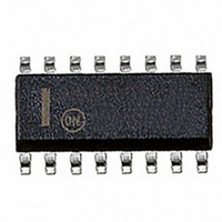
ADP3162JR-REEL ON Semiconductor, ADP3162JR-REEL Datasheet - Page 8

ADP3162JR-REEL
Manufacturer Part Number
ADP3162JR-REEL
Description
IC REG BUCK 5BIT 2PHASE 16-SOIC
Manufacturer
ON Semiconductor
Datasheet
1.ADP3162JRZ-REEL7.pdf
(12 pages)
Specifications of ADP3162JR-REEL
Rohs Status
RoHS non-compliant
Applications
Controller, Intel Tualatin
Voltage - Input
5V, 12V
Number Of Outputs
2
Voltage - Output
1.05 ~ 1.83 V
Operating Temperature
0°C ~ 70°C
Mounting Type
Surface Mount
Package / Case
16-SOIC (3.9mm Width)
Available stocks
Company
Part Number
Manufacturer
Quantity
Price
Company:
Part Number:
ADP3162JR-REEL
Manufacturer:
RTC
Quantity:
50 000
Part Number:
ADP3162JR-REEL
Manufacturer:
ADI/亚德诺
Quantity:
20 000
ADP3162
Selecting a Standard Inductor
The companies listed in Table III can provide design consul-
tation and deliver power inductors optimized for high power
applications upon request.
Coilcraft
(847) 639-6400; (800) 322-2645
http://www.coilcraft.com
Coiltronics
(561) 752-5000
http://www.coiltronics.com
Sumida Electric Company
(408) 982-9660
http://www.sumida.com
R
The value of R
current. The current comparator of the ADP3162 has a mini-
mum current limit threshold of 69 mV. Note that the 69 mV
value cannot be used for the maximum specified nominal cur-
rent, as headroom is needed for ripple current and tolerances.
The current comparator threshold sets the peak of the inductor
current yielding a maximum output current, I
twice the peak inductor current value less half of the peak-to-
peak inductor ripple current. From this the maximum value of
R
In this design example, 4 mΩ was chosen as the closest standard
value.
Once R
be calculated at the point where current limit is reached, using
the maximum current sense threshold of 89 mV:
At output voltages below 375 mV, the current sense threshold is
reduced to 58 mV maximum, and the ripple current is negli-
gible. Therefore, at dead short the maximum output current is
reduced to:
The capability of the resistor’s power rating should be checked
at maximum load current:
where:
I
OUT CL
SENSE
SENSE
(
R
I
P
I
OUT SC
SENSE RMS
R
SENSE
)
SENSE
SENSE
is calculated as:
= ×
2
(
Table III. Power Inductor Manufacturers
(
=
V
)
≤
has been chosen, the maximum output current can
CS CL
I
= ×
SENSE
R
SENSE RMS
I
(
)
2
2
V
O
SENSE
2
CS CL
)(
=
+
MAX
58
(
(
I
4
is based on the required maximum output
I
O
n
L RIPPLE
)
m
2
)(
(
mV
−
MIN
Ω
)
×
2
I
2
L RIPPLE
(
×
η
V
=
)
R
×
OUT
)
29
V
SENSE
=
IN
)
A
14
= ×
2
69
A
89
mV
4
+
m
mV
2
Ω
A
−
O
=
5 8
, which equals
.
4 08
.
A
=
m
38 7
Ω
.
A
(6)
(7)
(3)
(4)
(5)
In this formula, n is the number of phases, and η is the con-
verter efficiency, in this case assumed to be 85%. Combining
Equations 6 and 7 yields:
Output Resistance
Intel’s VRM 8.5 specification requires that the regulator
output voltage measured at the CPU pins drops when the
output current increases. The specified voltage drop corre-
sponds to a dc output resistance of:
The required dc output resistance can be achieved by terminating
the g
tion resistance that will yield the correct dc output resistance:
where n
the g
transconductance of the gm amplifier itself, and the factor of 2
is the result of the two-phase configuration.
Output Offset
Intel’s VRM 8.5 specification requires that at no load the output
voltage of the regulator module be offset to a higher value than
the nominal voltage corresponding to the VID code. The offset
is introduced by realizing the total termination resistance of the
gm amplifier with a divider connected between the REF pin and
ground. The resistive divider introduces an offset to the output
of the gm amplifier that, when reflected back through the gain
of the gm stage, accurately positions the output voltage near its
allowed maximum at light load. Furthermore, the output of the
gm amplifier sets the current sense threshold voltage. At no
load, the current sense threshold is increased by the peak of the
ripple current in the inductor and reduced by the delay between
sensing when the current threshold has been reached and when
the high side MOSFET actually turns off. These two factors are
combined with the inherent voltage (V
gm amplifier that commands a current sense threshold of 0 mV:
The divider resistors (R
can now be calculated assuming that the internal resistance of
the g
V
V
t
R
D
60
GNL
GNL
T
R
m
m
m
×
=
OUT
ns
amplifier with a resistor. The value of the total termina-
amplifier (R
amplifier to the PWM comparator CMP1, g
n
I
P
=
=
g
φ
is the division ratio from the output voltage signal of
× ×
R
n
m
V
×
1
SENSE
I
=
2 4
V
×
GNL
R
×
V
R
SENSE
R
+
ONL
OUT
=
0
SENSE
5 8
m
+
28
∆
.
Ω ×
−
I
OGM
2
I
×
×
O
L RIPPLE
A
V
A
2
(
n
OFL
2
I
×
25 1 194
=
) is 200 kΩ:
×
A
3 2
2 2
=
0 85 5
.
2
for the upper, and R
=
.
.
)
1 8
1 845
m
mmho
×
.
2
.
.
Ω ×
R
×
25 4
V
OUT
V
V
×
25
V
28
×
×
3 2
×
−
m
−
.
GNL0
n
A
4
1 755
Ω
I
5
.
m
m
−
V
Ω ×
Ω
), at the output of the
1
V
−
µ
IN
V
=
1 8
H
2
664
.
B
−
=
L
=
V
V
for the lower)
3 2
7 1
OUT
.
mW
.
×
m
m
k
is the
Ω
×
Ω
(10)
(8)
(9)


