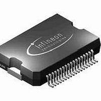
TLE6368G1 Infineon Technologies, TLE6368G1 Datasheet - Page 4

TLE6368G1
Manufacturer Part Number
TLE6368G1
Description
IC PS SYSTEM MULTI VOLT PDSO-36
Manufacturer
Infineon Technologies
Datasheet
1.TLE6368G1.pdf
(59 pages)
Specifications of TLE6368G1
Applications
Power Supply, Automotive Applications
Voltage - Input
5.5 ~ 60 V
Number Of Outputs
3
Voltage - Output
2.6V, 3.3V, 5V
Operating Temperature
-40°C ~ 150°C
Mounting Type
Surface Mount
Package / Case
DSO-36
Output Voltage
5.5 V
Output Current
1.5 A
Input Voltage Max
60 V
Mounting Style
SMD/SMT
Operating Temperature Range
- 40 C to + 150 C
Output Voltage Tolerance
+/- 10 %
For Use With
DEMOBOARDTLE6368IN - BOARD DEMO FOR TLE 6368
Lead Free Status / RoHS Status
Lead free / RoHS Compliant
Other names
SP000015046
SP000304810
TLE6368G1NT
TLE6368G1T
TLE6368G1XT
SP000304810
TLE6368G1NT
TLE6368G1T
TLE6368G1XT
Available stocks
Company
Part Number
Manufacturer
Quantity
Price
Part Number:
TLE6368G1A
Manufacturer:
INFINEON/英飞凌
Quantity:
20 000
Data Sheet
1.4
Pin No.
1,18,19,
36
2
3
4
5
6
7
8
9
10
Pin definitions and functions
Symbol
GND
CLK
CS
DI
DO
ERR
Q_STB
Q_T1
Q_T2
Q_T3
Function
Ground; to reduce thermal resistance place cooling areas on
PCB close to these pins. The GND pins are connected internally
to the heat slug at the bottom.
SPI Interface Clock input; clocks the shift register; CLK has an
internal active pull down and requires CMOS logic level
inputs;see also chapter SPI
SPI Interface chip select input; CS is an active low input; serial
communication is enabled by pulling the CS terminal low; CS
input should only be switched when CLK is low; CS has an
internal active pull up and requires CMOS logic level inputs ;see
also chapter SPI
SPI Interface Data input; receives serial data from the control
device; serial data transmitted to DI is a 16 bit control word with
the Least Significant Bit (LSB) being transferred first; the input
has an active pull down and requires CMOS logic level inputs; DI
will accept data on the falling edge of CLK-signal; see also
chapter SPI
SPI Interface Data output; this tristate output transfers
diagnosis data to the controlling device; the output will remain 3-
stated unless the device is selected by a low on Chip-Select CS;
see also the chapter SPI
Error output; push-pull output. Monitors failures in parallel to the
SPI diagnosis word, reset via SPI. ERR is an active low, latched
output.
Standby Regulator Output; the output is active even when the
buck regulator and all other circuitry is in off mode
Voltage Tracker Output T1 tracked to Q_LDO1; bypass with a
1µF ceramic capacitor for stability. It is switched on and off by
SPI command. Keep open, if not needed.
Voltage Tracker Output T2 tracked to Q_LDO1; bypass with a
1µF ceramic capacitor for stability. It is switched on and off by
SPI command. Keep open, if not needed.
Voltage Tracker Output T3 tracked to Q_LDO1; bypass with a
1µF ceramic capacitor for stability. It is switched on and off by
SPI command. Keep open, if not needed.
4
Rev. 2.2, 2006-12-01
TLE 6368 / SONIC


